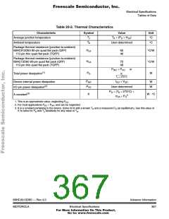
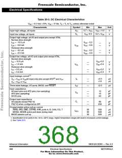
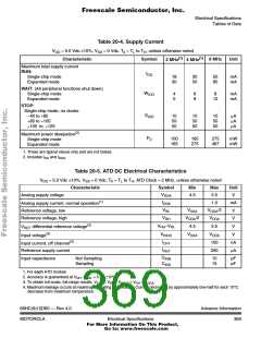
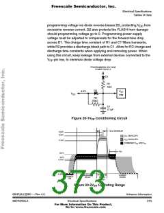
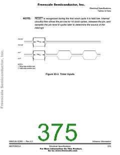
Freescale Semiconductor, Inc.
Electrical Specifications
Tables of Data
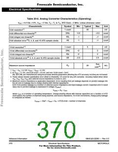
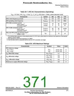
Table 20-7. ATD AC Characteristics (Operating)
V
= 5.0 Vdc ±10%, V = 0 Vdc, T = T to T , ATD Clock = 2 MHz, unless otherwise noted
SS A L H
DD
Characteristic
Symbol
Min
2.0
0.5
Max
8.0
2.0
Unit
MHz
MHz
f
MCU clock frequency (p-clock)
ATD operating clock frequency
PCLK
f
ATDCLK
ATD 8-Bit conversion period
clock cycles
conversion time
ATD 10-Bit conversion period
clock cycles
conversion time
n
18
9
32
16
cycles
µs
CONV8
(1)
t
(2)
(2)
CONV8
n
20
10
34
17
cycles
µs
CONV10
(1)
t
CONV10
(3)
Stop and ATD power up recovery time
VDDA = 5.0V
t
10
µs
SR
1. The minimum time assumes a final sample period of 2 ATD clock cycles while the maximum time assumes a final sample
period of 16ATD clocks.
2. This assumes an ATD clock frequency of 2.0MHz.
3. From the time ADPU is asserted until the time an ATD conversion can begin.
Table 20-8. ATD Maximum Ratings
Characteristic
Symbol
Value
Units
ATD reference voltage
V
V
≤ V
≥ V
V
V
RL
−0.3 to +6.5
−0.3 to +6.5
V
V
RH
RL
DDA
SSA
RH
V
V
V
differential voltage
differential voltage
differential voltage
|V −V
|
SSA
0.1
V
SS
DD
SS
V
V
−V
DDA
6.5
0.3
V
V
DD
−V
DDA
DD
|V −V
|
6.5
6.5
V
V
REF
RH
RL
|V −V
|
DDA
Reference to supply differential voltage
RH
68HC(9)12D60 — Rev 4.0
MOTOROLA
Advance Information
371
Electrical Specifications
For More Information On This Product,
Go to: www.freescale.com

 MOTOROLA [ MOTOROLA ]