Freescale Semiconductor, Inc.
Electrical Specifications
20.3 Tables of Data
(1)
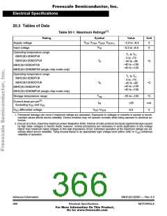
Table 20-1. Maximum Ratings
Rating
Supply voltage
Symbol
Value
Unit
V
V
, V
, V
V
−0.3 to +6.5
−0.3 to +6.5
DD DDA DDX, DDPLL
V
Input voltage
V
IN
Operating temperature range
68HC(9)12D60PV8
T to T
0 to +70
−40 to +85
–40 to +105
–40 to +125
L
H
68HC(9)12D60CPV8
T
°C
°C
A
68HC(9)12D60VPV8
68HC(9)12D60MPV8 (single chip mode only)
Operating temperature range
68HC(9)12D60FU8
T to T
0 to +70
−40 to +85
–40 to +105
–40 to +125
L
H
68HC(9)12D60CFU8
T
A
68HC(9)12D60VFU8
68HC(9)12D60MFU8 (single chip mode only)
T
Storage temperature range
−55 to +150
±25
°C
mA
V
stg
(2)
Current drain per pin
I
IN
Excluding V and V
DD
SS
V
differential voltage
V
−V
6.5
DD
DD DDX
1. Permanent damage can occur if maximum ratings are exceeded. Exposures to voltages or currents in excess of recom-
mended values affects device reliability. Device modules may not operate normally while being exposed to electrical ex-
tremes.
2. One pin at a time, observing maximum power dissipation limits. Internal circuitry protects the inputs against damage caused
by high static voltages or electric fields; however, normal precautions are necessary to avoid application of any voltage
higher than maximum-rated voltages to this high-impedance circuit. Extended operation at the maximum ratings can ad-
versely affect device reliability. Tying unused inputs to an appropriate logic voltage level (either GND or VDD) enhances
reliability of operation.
Advance Information
366
68HC(9)12D60 — Rev 4.0
MOTOROLA
Electrical Specifications
For More Information On This Product,
Go to: www.freescale.com

 MOTOROLA [ MOTOROLA ]