Freescale Semiconductor, Inc.
Pulse Width Modulator
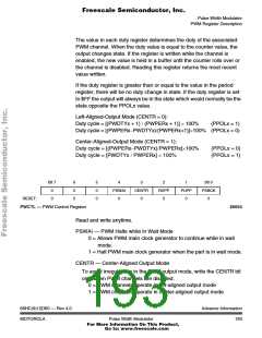
PWM Register Description
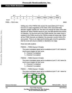
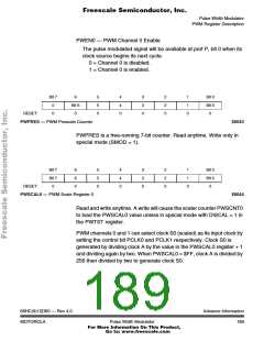
PWEN0 — PWM Channel 0 Enable
The pulse modulated signal will be available at port P, bit 0 when its
clock source begins its next cycle.
0 = Channel 0 is disabled.
1 = Channel 0 is enabled.
Bit 7
6
Bit 6
0
5
5
0
4
4
0
3
3
0
2
2
0
1
1
0
Bit 0
Bit 0
0
0
0
RESET:
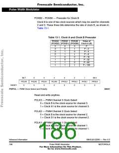
PWPRES — PWM Prescale Counter
$0043
PWPRES is a free-running 7-bit counter. Read anytime. Write only in
special mode (SMOD = 1).
Bit 7
Bit 7
0
6
6
0
5
5
0
4
4
0
3
3
0
2
2
0
1
1
0
Bit 0
Bit 0
0
RESET:
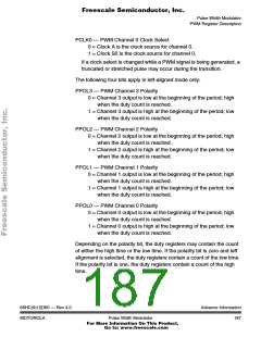
PWSCAL0 — PWM Scale Register 0
$0044
Read and write anytime. A write will cause the scaler counter PWSCNT0
to load the PWSCAL0 value unless in special mode with DISCAL = 1 in
the PWTST register.
PWM channels 0 and 1 can select clock S0 (scaled) as its input clock by
setting the control bit PCLK0 and PCLK1 respectively. Clock S0 is
generated by dividing clock A by the value in the PWSCAL0 register + 1
and dividing again by two. When PWSCAL0 = $FF, clock A is divided by
256 then divided by two to generate clock S0.
68HC(9)12D60 — Rev 4.0
MOTOROLA
Advance Information
Pulse Width Modulator
189
For More Information On This Product,
Go to: www.freescale.com

 MOTOROLA [ MOTOROLA ]