Freescale Semiconductor, Inc.
Pulse Width Modulator
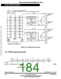
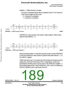
PWM Register Description
CON23 — Concatenate PWM Channels 2 and 3
When concatenated, channel 2 becomes the high-order byte and
channel 3 becomes the low-order byte. Channel 2 output pin is used
as the output for this 16-bit PWM (bit 2 of port P). Channel 3 clock-
select control bits determines the clock source. Channel 3 output pin
becomes a general purpose I/O.
0 = Channels 2 and 3 are separate 8-bit PWMs.
1 = Channels 2 and 3 are concatenated to create one 16-bit PWM
channel.
CON01 — Concatenate PWM Channels 0 and 1
When concatenated, channel 0 becomes the high-order byte and
channel 1 becomes the low-order byte. Channel 0 output pin is used
as the output for this 16-bit PWM (bit 0 of port P). Channel 1 clock-
select control bits determine the clock source. Channel 1 output pin
becomes a general purpose I/O.
0 = Channels 0 and 1 are separate 8-bit PWMs.
1 = Channels 0 and 1 are concatenated to create one 16-bit PWM
channel.
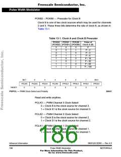
PCKA2 – PCKA0 — Prescaler for Clock A
Clock A is one of two clock sources which may be used for channels
0 and 1. These three bits determine the rate of clock A, as shown in
Table 13-1.
68HC(9)12D60 — Rev 4.0
MOTOROLA
Advance Information
Pulse Width Modulator
185
For More Information On This Product,
Go to: www.freescale.com

 MOTOROLA [ MOTOROLA ]