Freescale Semiconductor, Inc.
M
P
X
Y
8
0
2
0
A
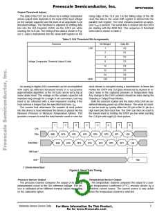
Output Threshold Adjust
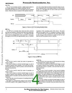
The state of the OUT pin is driven by a voltage comparator
whose output state depends on the level of the input voltage
on the sample capacitor and the level of an adjustable 8–bit
threshold voltage. The threshold is adjusted by shifting data
bits into the D/A Register (DAR) via the DATA pin while
clocking the CLK pin. The timing of this data is shown in Fig-
ure 6. Data is transferred into the serial shift register on the
rising edge of the CLK pin. On the falling edge of the 8th
clock the data in the serial shift register is latched into the
parallel DAR register. The DAR remains powered up when-
ever VDD is present. The serial data is clocked into the DATA
pin starting with the MSB first. This sequence of threshold
select bits is shown in Table 2.
Table 2. D/A Threshold Bit Assignments
Function
Bit Weight
Data Bit
D0
LSB
1
2
D1
4
D2
8
D3
Voltage Comparator Threshold Adjust (8 bits)
16
32
64
128
D4
D5
D6
MSB
D7
An analog to digital (A/D) conversion can be accomplished
with eight (8) different threshold levels in a successive
approximation algorithm; or the OUT pin can be set to trip at
some alarm level. The voltage on the sample capacitor will
maintain long enough for a single 8–bit conversion, but may
need to be refreshed with a new measured reading if the
clock stream is corrupted during a transmission. In these two
modes the DATA and CLK pins should not be clocked to re-
duce noise in the captured pressure or temperature data.
Any change in the DAR contents should be done during the
Standby or Output Read Modes.
Both the serial bit counter and the state of the DAR are un-
defined following power up of the device. The serial bit count-
er can be reset by cycling either the SO pin or the S1 pin to a
high level and then back low. The DAR can then be reset to
the lowest level by holding the DATA pin low while bursting
the CLK pin with eight (8) clock pulses.
read interval is longer than the specified hold time, tSH
.
The counter that determines the number of clock pulses
into the device is reset whenever the device is placed into the
Measure Pressure or Measure Temperature Modes. This
provides a means to reset the data transfer count in case the
1
2
3
4
5
6
7
8
CL K
D ata
M
S
B
B
I
T
6
B
I
T
5
B
I
T
4
B
I
T
3
B
I
T
2
B
I
T
1
L
S
B
S
e
r
i
a
l
D
a
t
a
M
S
B
B
I
T
6
B
I
T
5
B
I
T
4
B
I
T
3
B
I
T
2
B
I
T
1
L
S
B
D AR Lo ad
D A R
*
D
a
t
a
*
(
*
)
D
e
n
o
t
e
s
I
n
t
e
r
n
a
l
S
i
g
n
a
l
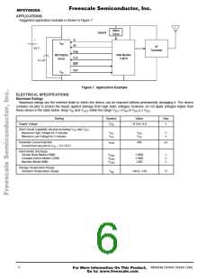
Figure 6. Serial Data Timing
Pressure Sensor Output
Temperature Sensor Output
The pressure channel compares the output of its analog
measurement circuit to the D/A reference voltage. The de-
vice is calibrated at two different nominal values depending
on the calibration option.
The temperature channel compares the output of a posi-
tive temperature coefficient (PTC) resistor driven by a
switched current source. The current source is only active
when the temperature channel is selected.
Motorola Sensor Device Data
5
For More Information On This Product,
Go to: www.freescale.com

 MOTOROLA [ MOTOROLA ]