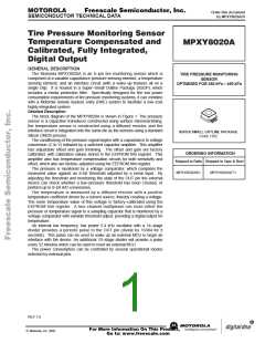
Freescale Semiconductor, Inc.
M
P
X
Y
8
0
2
0
A
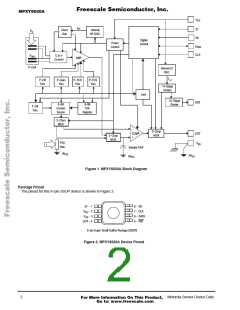
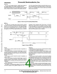
OUT Pin
The OUT pin normally provides a digital signal related to
the voltage applied to the voltage comparator and the
threshold level shifted into an 8–bit register from an external
device. When the device is placed in the standby mode the
OUT pin is driven high and will be clocked low when an over-
flow is detected from a clock divider (divide by 16384) driven
by the LFO. This allows the OUT pin to wake up an external
device such as an MCU.
O
U
T
2/ f
3
2 / f
LF
L
F
O
O
Op e r at io n
M easu r e
S tan d by
Me a sur e
S ec
Wa ke U p
Figure 4. Pulse on OUT Pin During Standby Mode
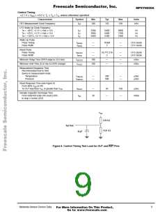
RST Pin
The RST pin is normally driven high and will be clocked
low when an overflow is detected from total clock divider (di-
vide by 16,777,216) driven by the LFO. This allows the RST
pin to reset an external device such as an MCU. This pulse
will appear on the RST pin approximately every 52 minutes
regardless of the operating mode of the device. The pulse
lasts for two cycles of the LFO oscillator as shown in Figure
5. Since the RST pin is clocked from the same divider string
as the OUT pin, there will also be a pulse on the OUT pin
when the RST pin pulses every 52 minutes.
2/ f
L F O
OU T
R ST
2/ f
L
F
O
Sta n db y
≈
≈
3
S
e
c
≈
5
2
M
i
n
u
t
e
s
Figure 5. Pulse on RST Pin
S0 Pin
DATA Pin
The S0 pin is used to select the mode of operation as
shown in Table 1.
The DATA pin is the serial data in (SDI) function for setting
the threshold of the voltage comparator.
The S0 pin contains an internal Schmitt trigger as part of
its input to improve noise immunity. The S0 pin has an inter-
nal pull–down device in order to provide a low level when the
pin is left unconnected.
The DATA pin contains an internal Schmitt trigger as part
of its input to improve noise immunity. This pin has an inter-
nal pull–down device to provide a low level when the pin is
left unconnected.
S1 Pin
CLK Pin
The S1 pin is used to select the mode of operation, as
shown in Table 1.
The S1 pin contains an internal Schmitt trigger as part of
its input to improve noise immunity. This pin has an internal
pulldown device to provide a low level when the pin is left un-
connected.
The S1 pin also serves the purpose of enabling factory trim
and test of the device.
The higher VPP programming voltage for the internal EE-
PROM trim register is also supplied through the S1 pin.
The CLK pin is used to provide a clock used for loading
and shifting data into the DATA pin. The data on the DATA pin
is clocked into a shift register on the rising edge of the CLK
pin signal. The data is transferred to the D/A Register on the
eighth falling edge of the CLK pin. This protocol may be han-
dled by the SPI or SIOP serial I/O function found on some
MCU devices.
The CLK pin contains an internal Schmitt trigger as part of
its input to improve noise immunity. The CLK pin has an inter-
nal pulldown device to provide a low level when the pin is left
unconnected.
4
Motorola Sensor Device Data
For More Information On This Product,
Go to: www.freescale.com

 MOTOROLA [ MOTOROLA ]