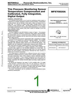
Freescale Semiconductor, Inc.
M
P
X
Y
8
0
2
0
A
Operating Modes
The device has several operating modes dependent on
the applied voltages to the S1 and S0 pins as shown in Table
1. In all the modes listed the channel multiplexers, D/A Reg-
ister, LFO, and the output pulse dividers will always be pow-
ered up as long as there is a voltage source connected to the
sample capacitor before powering down the measuring cir-
cuitry.
NOTE: All of the EEPROM trim bits will be powered up re-
gardless of whether the pressure or temperature measuring
circuitry is activated.
V
DD pin.
NOTE: If the voltage on the S1 pin exceeds 2.5 times the
voltage on the VDD pin the device will be placed into its Trim/
Test Mode.
When only the S0 pin is at a logic one the pressure mea-
suring circuit in the device is powered up and the pressure
output signal is connected to the sample capacitor through a
multiplexer. When the S0 pin returns to the low state the mul-
tiplexer will first turn off to store the signal on the sample ca-
pacitor before powering down the measuring circuitry.
When only the S1 pin is at a logic one the temperature
measuring circuit in the device is powered up and the tem-
perature output signal is connected to the sample capacitor
through a multiplexer. When the S1 pin returns to the low
state the multiplexer will first turn off to store the signal on the
NOTE: If the VDD supply source is switched off in order to
reduce current consumption, it is important that all input pins
be driven LOW to avoid powering up the device.
If any input pin (S1, S0, DATA, or CLK) is driven HIGH
while the VDD supply is switched off, the device may be pow-
ered up through an ESD protection diode. In such a case, the
effective VDD voltage will be about 0.3 V less than the voltage
applied to the input pin, and the full device IDD current will be
drawn from the device driving input.
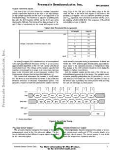
Table 1. Operating Modes
Circuitry Powered
Serial Data
Counter
Pressure
Measure
System
Temp
Measure
System
A/D
Output
Comp.
LFO
Oscill.
S1
S0
Operating Mode
0
0
1
1
0
1
0
1
Standby/Reset
OFF
ON
OFF
OFF
ON
OFF
OFF
OFF
ON
ON
ON
ON
ON
ACTIVE
RESET
RESET
ACTIVE
Measure Pressure
Measure Temperature
Output Read
OFF
OFF
OFF
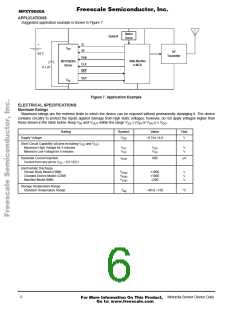
Pin Functions
The following paragraphs give a description of the general
function of each pin.
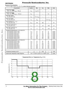
ground. The control IC operates from a single power supply.
Therefore, the conductors to the power supply should be
connected to the VDD and VSS pins and locally decoupled as
shown in Figure 3.
VDD and VSS Pins
Power is supplied to the control IC through VDD and VSS
.
V
DD is the positive supply and VSS is the digital and analog
M
P
X
Y
8
0
2
0
A
To O t he r V L oa d s
D D
V
D
V
D D
D
0 .1 µF
T
o
P
o
w
e
r
S
u
p
p
l
y
V
S
V
S S
S
To O t he r V Re t ur ns
S
S
Figure 3. Recommended Power Supply Connections
Motorola Sensor Device Data
3
For More Information On This Product,
Go to: www.freescale.com

 MOTOROLA [ MOTOROLA ]