Freescale Semiconductor, Inc.
M P XY 8 020 A
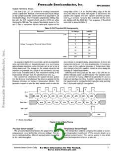
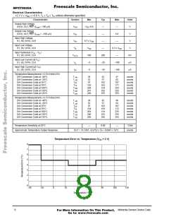
Control Timing
+2.1 V ≤ VDD ≤ +3.6 V, TL ≤ TA ≤ TH, unless otherwise specified.
Characteristic
Symbol
Min
Typ
Max
Units
HFO Measurement Clock Frequency
f
HF
100
135
150
kHz
LFO Wake Up Clock Frequency
Ta = –40°C, +2.1V ≤ Vdd ≤ +3.6
Ta = +25°C, +2.1V ≤ Vdd ≤ +3.6
Ta = +125°C, +2.1V ≤ Vdd ≤ +3.6
f
LF
f
LF
f
LF
3300
3900
3800
5400
5400
5300
8000
7700
7000
Hz
Hz
Hz
Wake Up Pulse
Pulse Timing
Pulse Width
t
t
—
—
16384
2
—
—
LFO clocks
LFO clocks
WAKE
WPW
Reset Pulse
Pulse Timing
Pulse Width
t
t
—
—
16,777,216
2
LFO clocks
LFO clocks
—
—
RESET
t
RPW
Minimum Setup Time (DATA edge to CLK rise)
Minimum Hold Time (CLK rise to DATA change)
100
100
—
—
—
—
nSec
nSec
SETUP
t
HOLD
Measurement Response Time
Recommended time to hold
device in measurement mode
Temperature
t
—
—
200
500
—
—
µSec
µSec
TMEAS
t
PMEAS
Pressure
Read Response Time (see Figure 8)
From 90% V on S0
DD
To OUT less than V or greater than V
t
READ
—
50
—
100
—
µSec
OL
OH
Sample Capacitor Discharge Time
From initial full scale D/A count (255)
to drop 2 counts (253)
t
20
mSec
SH
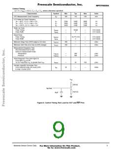
V
D
D
6 .3 2 Ωk
T
e
s
t
P
o
i
n
t
1 0. 9 1 Ωk
5
0
p
F
Figure 8. Control Timing Test Load for OUT and RST Pins
Motorola Sensor Device Data
9
For More Information On This Product,
Go to: www.freescale.com

 MOTOROLA [ MOTOROLA ]