Freescale Semiconductor, Inc.
Given the brief example on how aliasing can occur, how
DEMONSTRATION OF ALIASING
does the accelerometer relate to aliasing? To answer this
question, a brief summary on how the accelerometer works is
in order.
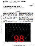
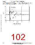
Underzeroaccelerationconditionsa100mV
signalwas
rms
injected onto the power supply line of 5.0 Vdc. The frequency
of the injected signal was tuned in to produce an alias in the
accelerometer’s passband. Figures 3 and 4 show the
difference in output when a high frequency signal is not and is
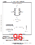
The accelerometer is a two chip acceleration sensing
solution. The first chip is the acceleration transducer, termed
G–Cell, constructed by Micro Electro–Mechanical Systems
(MEMS) technology. The G–Cell is a two capacitor element
where the capacitors are in series and share a common center
plate. The deflection in the center plate changes the capaci-
tanceofeachcapacitorwhichismeasuredbythesecondchip,
termed control chip.
The control chipperformsthesignalconditioning(amplifica-
tion, filtering, offset level shift) function in the system. This chip
measures the G–Cell output using switched capacitor tech-
niques. By the nature of switched cap techniques, the system
present on the V
pin of the accelerometer.
CC
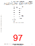
1.0E+0
1.0E–1
1.0E–2
1.0E–3
1.0E–4
1.0E–5
1.0E–6
V
out
SAMPLING
FREQUENCY
is a sampled data system operating at sampling frequency f .
s
The filter is switched capacitor, 4–pole Bessel implementation
with a –3 dB frequency of 400 Hz.
As a sampled data system, the accelerometer is not immune
to signal aliasing. However, given the accelerometer’s internal
filter, aliased signals will only appear in the output passband
1.0E–7
41.0
41.2
41.4
41.6
41.8
42.0
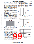
wheninputsignalsareintherange|n• f –f
|≤f .Where
s
signal BW
FREQUENCY (kHz)
f is the sampling rate, f
is the input signal frequency, f
s
Signal
BW
is the filter bandwidth and n is a positive integer to account for
all harmonics. The graphical representation is shown in Figure
(a)
2. The bounds can be extended beyond f
free output.
to ensure an alias
BW
1.0E+0
1.0E–1
1.0E–2
1.0E–3
1.0E–4
1.0E–5
1.0E–6
V
CC
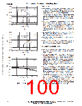
KEEP OUT ZONE
SAMPLING
FREQUENCY
1.0E–7
41.0
Hz
41.2
41.4
41.6
41.8
42.0
n*f – f
s BW
n*f
s
n*f + f
s BW
FREQUENCY (kHz)
Figure 2. Input signal frequency range where a signal
will be produced in the output passband.
(b)
1.0E+0
1.0E–1
1.0E–2
1.0E–3
1.0E–4
1.0E–5
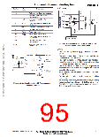
ACCELEROMETER INPUT SIGNALS
V
out
The accelerometer is a ratiometric electro–mechanical
transducer. Therefore, the input signals to the device are the
acceleration and the input power source.
The acceleration input is limited in frequency bandwidth by
the geometry of the sensing, packaging, and mounting
structures that define the resonant frequency and response.
This response is in the range of 10 kHz, however, the practical
range is less than 600 Hz for most mechanical systems.
Therefore, aliasing an acceleration signal is unlikely.
The power input signal is ideally dc. However, dependingon
the application system architecture, the power supply line can
be riddled with high frequency components. For example, dc
to dc converters can operate with switching frequencies
between 20 kHz and 200 kHz. This range encompasses the
sampling rate of the accelerometer and point to the power
source as the culprit in producing aliased signal.
1.0E–6
0
200
400
600
800
1000
FREQUENCY (Hz)
(c)
Figure 3. Normal Waveforms
Motorola Sensor Device Data
www.motorola.com/semiconductors
2–63
For More Information On This Product,
Go to: www.freescale.com

 MOTOROLA [ MOTOROLA ]