Freescale Semiconductor, Inc.
PCB Layout
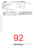
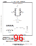
Pin No.
Pin
Description
Name
STATUS
P1
1 thru 3
4
—
—
Redundant Vss. Leave unconnected.
ST
P0
No internal connection. Leave
unconnected.
X
OUT
A/D IN
R
C
C
1 kΩ
0.01 µF
0.01 µF
5
6
ST
Logic input pin used to initiate
self–test.
V
SS
Y
A/D IN
OUT
R
C
0.1 µF
X
Output voltage of the accelerometer.
X Direction.
1 kΩ
OUT
V
SS
V
DD
C
0.1 µF
7
8
STATUS
Logic output pin to indicate fault.
The power supply ground.
Power supply input.
V
DD
V
RH
V
SS
C
0.1 µF
9
V
DD
10
11
AV
Power supply input (Analog).
DD
Y
OUT
Output voltage of the accelerometer.
Y Direction.
POWER SUPPLY
12 thru 16
17 thru 20
—
—
Used for factory trim. Leave
unconnected.
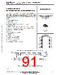
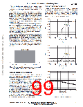
Figure 5. Recommend PCB Layout for Interfacing
Accelerometer to Microcontroller
No internal connection. Leave
unconnected.
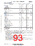
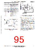
NOTES:
•
•
•
Use a 0.1 µF capacitor on V
source.
to decouple the power
DD
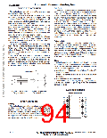
7
MMA3201D
STATUS
V
DD
Physical coupling distance of the accelerometer to the mi-
crocontroller should be minimal.
LOGIC
INPUT
5
9
ST
R1
1 kΩ
X OUTPUT
SIGNAL
6
OUT
V
X
Place a ground plane beneath the accelerometer to reduce
noise, the ground plane should be attached to all of the
open ended terminals shown in Figure 4.
DD
C1
0.1 µF
10
8
C2
0.01 µF
AV
DD
•
Use an RC filter of 1 kΩ and 0.01 µF on the outputs of the
accelerometer to minimize clock noise (from the switched
capacitor filter circuit).
V
SS
R2
1 kΩ
Y OUTPUT
SIGNAL
11
Y
OUT
•
•
•
PCB layout of power and ground should not couple power
supply noise.
C3
0.01 µF
Accelerometer and microcontroller should not be a high
current path.
A/Dsamplingrateandanyexternalpowersupplyswitching
frequency should be selected such that they do not inter-
fere with the internal accelerometer sampling frequency.
This will prevent aliasing errors.
Figure 4. SOIC Accelerometer with Recommended
Connection Diagram
Motorola Sensor Device Data
www.motorola.com/semiconductors
Go to: www.freescale.com
2–59
For More Information On This Product,

 MOTOROLA [ MOTOROLA ]