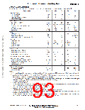
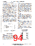
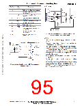
Freescale Semiconductor, Inc.
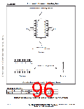
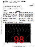
Surface mount board layout is a critical portion of the total
footprint, the packages will self–align when subjected to a
solder reflow process. It is always recommended to design
boards with a solder mask layer to avoid bridging and short-
ing between solder pads.
design. The footprint for the surface mount packages must
be the correct size to ensure proper solder connection inter-
face between the board and the package. With the correct
0.050 in.
1.27 mm
0.380 in.
9.65 mm
0.024 in.
0.610 mm
0.080 in.
2.03 mm
Figure 6. Footprint SOIC–20 (Case 475A–01)
Motorola Sensor Device Data
www.motorola.com/semiconductors
2–61
For More Information On This Product,
Go to: www.freescale.com

 MOTOROLA [ MOTOROLA ]