Freescale Semiconductor, Inc.
1.0E+0
1.0E–1
1.0E–2
Points to note:
•
•
•
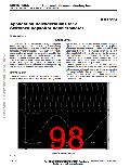
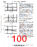
Undercleandcbias,V andV ,Figures3aand3bhave
out CC
V
out
INJECTED SIGNAL
FREQUENCY
a signal component at the sampling rate. This is due to
switched capacitor currents coupling through finite power
supply source impedances and PCB paracitics.
SAMPLING
FREQUENCY
Thelowfrequencyoutputspectrum, Figure3c, displaysthe
internal lowpass filter characteristics. (The filter and sam-
pling characteristics are sometimes useful in system de-
bugging.)
1.0E–3
1.0E–4
1.0E–5
1.0E–6
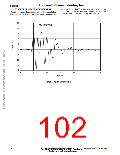
When an ac component is superimposed onto V
CC
near
the sampling frequency, as shown in Figure 4b, the output
will contain the original signal plus a mirrored signal about
the sampling frequency, shown in Figure 4a. Signals on the
41.0
41.2
41.4
41.6
41.8
42.0
FREQUENCY (kHz)
V
line will appear at the output due to the ratiometric
CC
characteristic of the accelerometer and will be one half the
amplitude.
(a)
•
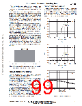
As a result of sampling, the output waveform of Figure 4c
is produced where the injected high frequency signal has
now produced a signal in the passband.
1.0E+0
1.0E–1
1.0E–2
1.0E–3
1.0E–4
1.0E–5
1.0E–6
1.0E–7
V
CC
INJECTED SIGNAL
FREQUENCY
•
•
Harmonics of the aliased signal in the pass band are also
shown in Figure 4c.
Aliased signals in the passband will be amplified versions
of the injected signals. This is due to the signal conditioning
circuitry in the accelerometer that includes gain.
SAMPLING
FREQUENCY
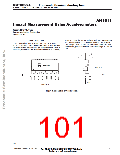
ALIASING AVOIDANCE KEYS
•
Use a linear regulated power source when feasible. Linear
regulators have excellent power supply rejection offering a
stable dc source.
41.0
41.2
41.4
41.6
41.8
42.0
FREQUENCY (kHz)
(b)
•
If using a switching power supply, ensure that the switching
frequency is not close to the accelerometer sampling fre-
quency or its harmonics. Noting that the accelerometer will
gain the aliasing signal, it is desirable to keep frequencies
at least 4 kHz away from the sampling frequency and its
harmonics. 4 kHz is one decade from the –3 dB frequency,
therefore any signals will be sufficiently attenuated by the
internal 4–pole lowpass filter.
1.0E+0
1.0E–1
1.0E–2
1.0E–3
1.0E–4
1.0E–5
1.0E–6
V
out
•
•
Proper bias decoupling will aid in noise reduction from oth-
er sources. With dense surface mount PCB assemblies, it
is often difficult to place and route decoupling components.
However, the accelerometer is not like a typical logic de-
vice. A little extra effort on decoupling goes a long way.
Good PCB layout practices should always be followed.
Proper system grounding is essential. Parasitic capaci-
tance and inductance could prove to be troublesome, par-
ticularly during EMC testing. Signal harmonics and
sub–harmonicsplayasignificantroleinintroducingaliased
signals. Clean layouts minimize the effects of parasitics
and thus signal harmonics and sub–harmonics.
0
200
400
600
800
1000
FREQUENCY (Hz)
(c)
Figure 4. Aliasing Comparison
2–64
www.motorola.com/semiconductors
Motorola Sensor Device Data
For More Information On This Product,
Go to: www.freescale.com

 MOTOROLA [ MOTOROLA ]