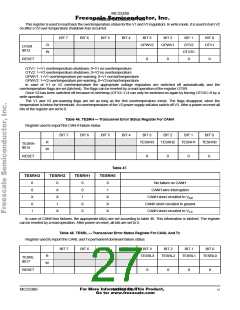
MC33389
Freescale Semiconductor, Inc.
APPLICATION
Sleep Mode Activation
The SBC then enters sleep mode. It will wake up after the
Once in sleep mode, the SBC turns off V1 and V2
regulator. Thus the micro controller can not run any mode.
in order to have it run again, the SBC should enable and
turn on V1, and this is achieve by an SBC wake up event.
Several options are available to wake up the SBC and the
application and have the micro controller in run mode.
Some wake up are selectable, some are always active in
sleep mode.
time period selected in the CYTCR register.
Sleep Mode Enter With Cyclic Sense
To enter sleep mode and activate the cyclic sense wake
up the following register must be written:
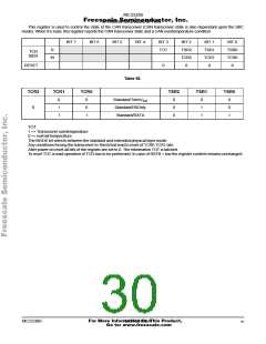
- Write to V3R register, data 1010, this set the VI2V3 and
CYS bits to 1.
- Write to CYTCR register the desired cyclic sense period.
(This sets the time the SBC will wait in sleep mode to turn on
V3 and sense the Lx inputs).
- Wake up from CAN interface and wake up from SPI
(CSB) are always active.
- Wake up from L0/L1/L2 inputs, with and without cyclic
sense and the FWU (Forced Wake Up) are selectable. The
selection must be done while the SBC is in Normal or Standby
mode, and prior to enter sleep mode.
- Write to WUICR bits 0 and 1 to select the edge sensitivity
for the Lx inputs.
- Write to MCR register: data SLEEP (100)
- Write to MCVR register: data SLEEP (100)
The SBC then enters sleep mode. It will periodically turn
on V3 and while V3 is on, sample the level of the Ls inputs.
If any of the 3 Lx inputs is in the correct state for two
consecutive samples, SBC will wake up. If not, it will stay in
sleep mode. (refer to device description for detail).
General Condition To Enter Sleep Mode
In order to make sure the SBC enters the sleep mode, and
in addition to the write into MCR and MCVR register, all
previous wake up conditions must have been cleared. To
clear a wake up condition requires that the appropriate
register is read.
Sleep Mode Enter With Direct Lx Input Wake Up
To enter sleep mode and activate the direct wake up from
the Lx inputs, the following register must be written:
- Write to V3R register, data 0000), this clear VI2V3 bit.
- Write to WUICR bits 0 and 1 to select the edge sensitivity
for the Lx inputs.
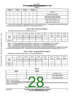
After an SBC power up from “zero” (battery power up or
cold start), the following registers must be read:
- WUICR: possible wake up event report from CAN bus
- RSR: report a V1 undervoltage
- VSSR: reports a Vbat fail flag
Once these read operation are done, the wake up
conditions or flag are reset.
- Write to MCR register: data SLEEP (100)
- Write to MCVR register: data SLEEP (100)
The SBC then enters sleep mode. It will wake up as soon
as any of the Lx input read the correct state.
The VSSR register bit VBSR0 can be used to determined
if the SBC has experience a loss of battery voltage.
After an SBC wake up from “sleep mode” the following
registers indicate the wake up source and must be cleared in
order to allow the SBC to enter sleep mode again:
- WUICR: wake up event report for CAN or SPI buses.
- WUISR: Wake up event report for the L0/L1/L2 inputs.
- RSR: report a V1 undervoltage
Figure 59. Typical Sleep Current vs Temp and Batt
180
160
140
120
100
- VSSR: reports a Vbat fail flag
- etc
The paragraphs below describe the write operation to be
done for the several sleep mode and wake up control options.
In addition to FWU, cyclic sense and direct wake up, the
CAN and SPI wake will always be activated.
Sleep Mode With CAN And SPI Wake Up
The enter sleep mode and activate the only the CAN or
SPI wake up, no dedicated wake up condition must be done.
In sleep mode the SBC has CAN and SPI wake up always
active. To enter sleep mode in this case, while the SBC is in
normal or standby mode:
80
16V
60
12V
6V
40
-50
- Write to V3R register: data 0000 (this clear the bit WI2V3
which is set to1 after reset).
-25
0
25
50
75
100
125 150
- Write to MCR register: data SLEEP (100)
TEMPERATURE (°C)
- Write to MCVR register: data SLEEP (100)
The SBC then enters sleep mode.
Voltage
Sleep Mode Enter With Forced Wake Up
To enter sleep mode and activate the forced wake up the
following register must be written:
- Write to V3R register, data 0100), this set the FWU bit to 1.
- Write to CYTCR register the desired wake up time. (This
sets the time the SBC will stay in sleep mode).
- Write to MCR register: data SLEEP (100)
- Write to MCVR register: data SLEEP (100)
For More Information On This Product,
MC33389
MOTOROLA
31
Go to: www.freescale.com

 MOTOROLA [ MOTOROLA ]