MITSUBISHI MICROCOMPUTERS
3827 Group
SINGLE-CHIP 8-BIT CMOS MICROCOMPUTER
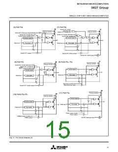
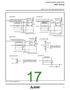
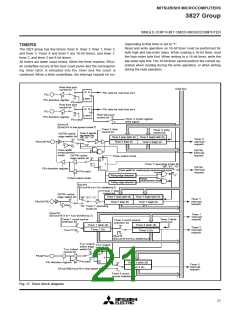
(18) Port P61
(19) Port P62
Pull-up control
Pull-up control
Synchronous clock selection bit
P61/SOUT2 P-channel output disable bit
Serial I/O2 transmit completion signal
Synchronous clock selection bit
Serial I/O2 port selection bit
Synchronous clock output pin
selection bit
Serial I/O2 port selection bit
Direction register
Direction register
Data bus
Port latch
Data bus
Port latch
Serial I/O2 output
Serial I/O2 clock output
A-D conversion input
Serial I/O2 clock input
Analog input pin selection bit
A-D conversion input
Analog input pin selection bit
(20) Port P63
Pull-up control
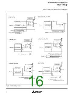
(21) COM0–COM3
Synchronous clock selection bit
Serial I/O2 port selection bit
Synchronous clock output pin selection bit
VL3
Direction register
VL2
VL1
Data bus
Port latch
The gate input signal of each
transistor is controlled by the
LCD duty ratio and the bias
value.
Serial I/O2 clock output
VSS
A-D conversion input
Analog input pin selection bit
(23) Port P70
(22) SEG0–SEG17
Direction register
VL2/VL3
The voltage applied to the sources of
P-channel and N-channel transistors
is the controlled voltage by the bias
value.
Port latch
Data bus
VL1/VSS
INT0 input
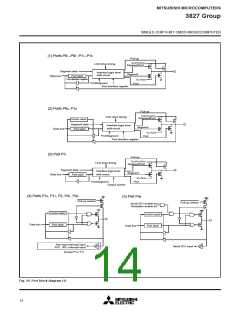
Fig. 13 Port block diagram (4)
17

 MITSUBISHI [ Mitsubishi Group ]