MITSUBISHI MICROCOMPUTERS
M37270MF-XXXSP
M37270EF-XXXSP, M37270EFSP
SINGLE-CHIP 8-BIT CMOS MICROCOMPUTER with CLOSED CAPTION DECODER
and ON-SCREEN DISPLAY CONTROLLER
When the relevant bit is cleared to “0,” determination is made of
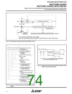
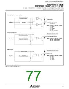
INTERRUPT INTERVAL DETERMINATION
FUNCTION
the interval of a positive polarity (rising transition) ; when the bit is
set to “1,” determination is made of the interval of a negative po-
larity (falling transition).
The M37270MF-XXXSP incorporates an interrupt interval determi-
nation circuit. This interrupt interval determination circuit has an 8-bit
binary up counter as shown in Figure 83. Using this counter, it deter-
mines an interval or a pulse width on the INT1 or INT2 (refer to Fig-
ure 85).
4. The reference clock is selected by using bit 1 of the interrupt inter-
val determination control register. When the bit is cleared to “0,” a
32µs clock is selected ; when the bit is set to “1,” a 16µs clock is
selected (based on an oscillation frequency of 8MHz in either case).
5. Simultaneously when the input pulse of the specified polarity
(rising or falling transition) occurs on the INT1 pin (or INT2 pin),
the 8-bit binary up counter starts counting up with the selected
reference clock (32µs or 16µs).
The following describes how the interrupt interval is determined.
1. The determination mode is selected by using bit 5 of the interrupt
interval determination control register (address 021216). When this
bit is set to “0,” the interrupt interval determination mode is se-
lected; when the bit is set to “1,” the pulse width determination
mode is selected.
6. Simultaneously with the next input pulse, the value of the 8-bit
binary up counter is loaded into the interrupt interval determina-
tion register (address 021116) and the counter is immediately re-
set (“0016”). The reference clock is input in succession even after
the counter is reset, and the counter restarts counting up from
“0016”.
2. The interrupt input to be determined (INT1 input or INT2 input) is
selected by using bit 2 in the interrupt interval determination con-
trol register (address 021216). When this bit is cleared to “0,” the
INT1 input is selected ; when the bit is set to “1,” the INT2 input is
selected.
3. When the INT1 input is to be determined, the polarity is selected
by using bit 3 of the interrupt interval determination control
register ; when the INT2 input is to be determined, the polarity is
selected by using bit 4 of the interrupt interval determination
control register.
7. When count value “FE16” is reached, the 8-bit binary up counter
stops counting. Then, simultaneously when the next reference
clock is input, the counter sets value “FF16” to the interrupt inter-
val determination register. The reference clock is generated by
setting bit 0 of the PWM mode register 1 to “0.”
73

 MITSUBISHI [ Mitsubishi Group ]