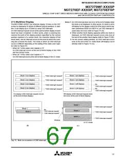
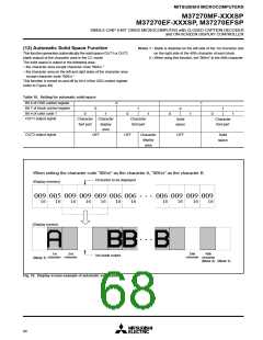
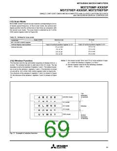
MITSUBISHI MICROCOMPUTERS
M37270MF-XXXSP
M37270EF-XXXSP, M37270EFSP
SINGLE-CHIP 8-BIT CMOS MICROCOMPUTER with CLOSED CAPTION DECODER
and ON-SCREEN DISPLAY CONTROLLER
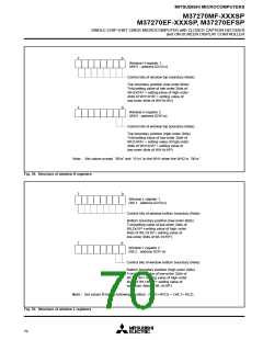
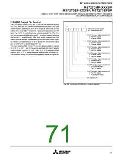
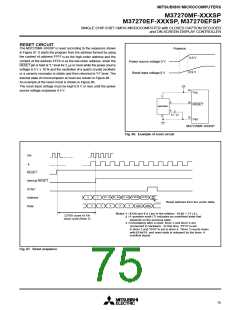
(15) OSD Output Pin Control
The OSD output pins R, G, B, and OUT1 can also function as ports
P52, P53, P54 and P55. Set the corresponding bit of the OSD port
control register (address 00CB16) to “0” to specify these pins as OSD
output pins, or set it to “1” to specify it as a general-purpose port P5
pins. The OUT2, I1, and I2 can also function as port P10, P15, P16.
Set the corresponding bit of the port P1 direction register (address
00C316) to “1” (output mode). After that, switch between the OSD
output function and the port function by the OSD port control regis-
ter. Set the corresponding bit to “1” to specify the pin as OSD output
pin, or set it to “0” to specify as port P1 pin.
7
0
0
OSD port control register
(PF : address 00CB16
)
Port P1
0 : Port P1
1 : I1 signal output
5
output signal selection bit
5
output
Port P1
6
output signal selection bit
0 : Port P16 output
1 : I2 signal output
The input polarity of the HSYNC, VSYNC and output polarity of signals
R, G, B, I1, I2, OUT1 and OUT2 can be specified with the I/O polarity
control register (address 021716) . Set a bit to “0” to specify positive
polarity; set it to “1” to specify negative polarity (refer to Figure 61).
The structure of the OSD port control register is shown in Figure 80.
Port P5
0 : R signal output
1 : Port P5
2
output signal selection bit
2 output
Port P5 output signal selection bit
0 : G signal output
1 : Port P5 output
3
3
Port P54 output signal selection bit
0 : B signal output
1 : Port P5 output
4
Port P55 output signal selection bit
0 : OUT1 signal output
1 : Port P5 output
5
Port P1
0 : Port P1
0
output signal selection bit
output
0
1 : OUT2 signal output
Fix this bit to “0.”
Fig. 80. Structure of OSD port control register
71

 MITSUBISHI [ Mitsubishi Group ]