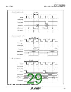
Mitsubishi microcomputers
M16C / 61 Group
SINGLE-CHIP 16-BIT CMOS MICROCOMPUTER
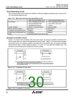
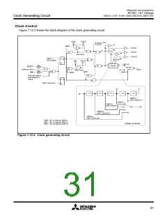
Clock Generating Circuit
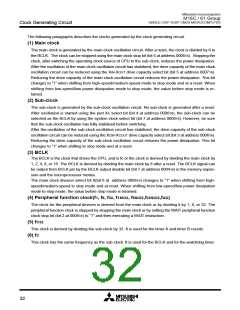
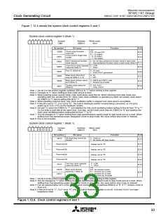
Figure 1.12.4 shows the system clock control registers 0 and 1.
System clock control register 0 (Note 1)
b7 b6 b5 b4 b3 b2 b1 b0
Symbol
CM0
Address
000616
When reset
4816
Bit symbol
CM00
Bit name
Function
R W
b1 b0
Clock output function
select bit
(Valid only in single-chip
mode)
0 0 : I/O port P5
0 1 : f
1 0 : f
1 1 : f32 output
7
C
output
output
8
CM01
CM02
CM03
WAIT peripheral function
clock stop bit
0 : Do not stop peripheral function clock in wait mode
1 : Stop peripheral function clock in wait mode (Note 8)
X
CIN-XCOUT drive capacity 0 : LOW
select bit (Note 2)
1 : HIGH
Port X
C
select bit
0 : I/O port
1 : XCIN-XCOUT generation
CM04
CM05
Main clock (XIN-XOUT
stop bit (Note 3, 4, 5)
)
0 : On
1 : Off
Main clock division select 0 : CM16 and CM17 valid
CM06
CM07
bit 0 (Note 7)
1 : Division by 8 mode
System clock select bit
(Note 6)
0 : XIN, XOUT
1 : XCIN, XCOUT
Note 1: Set bit 0 of the protect register (address 000A16) to “1” before writing to this register.
Note 2: Changes to “1” when shiffing to stop mode and at a reset.
Note 3: When entering power saving mode, main clock stops using this bit. When returning from stop mode and
operating with XIN, set this bit to “0”. When main clock oscillation is operating by itself, set system clock select
bit (CM07) to “1” before setting this bit to “1”.
Note 4: When inputting external clock, only clock oscillation buffer is stopped and clock input is acceptable.
Note 5: If this bit is set to “1”, XOUT turns “H”. The built-in feedback resistor remains being connected, so XIN turns
pulled up to XOUT (“H”) via the feedback resistor.
Note 6: Set port Xc select bit (CM04) to “1” and stabilize the sub-clock oscillating before setting to this bit from “0” to “1”.
Do not write to both bits at the same time. And also, set the main clock stop bit (CM05) to “0” and stabilize the
main clock oscillating before setting this bit from “1” to “0”.
Note 7: This bit changes to “1” when shifting from high-speed/medium-speed mode to stop mode and at a reset. When
shifting from low-speed/low power dissipation mode to stop mode, the value before stop mode is retained.
Note 8: fC32 is not included.
System clock control register 1 (Note 1)
b7 b6 b5 b4 b3 b2 b1 b0
Symbol
CM1
Address
000716
When reset
2016
0
0
0
0
Bit symbol
CM10
Bit name
Function
R W
All clock stop control bit
(Note4)
0 : Clock on
1 : All clocks off (stop mode)
Reserved bit
Always set to “0”
Reserved bit
Reserved bit
Reserved bit
Always set to “0”
Always set to “0”
Always set to “0”
X
IN-XOUT drive capacity
0 : LOW
1 : HIGH
CM15
select bit (Note 2)
b7 b6
Main clock division
select bit 1 (Note 3)
0 0 : No division mode
0 1 : Division by 2 mode
1 0 : Division by 4 mode
1 1 : Division by 16 mode
CM16
CM17
Note 1: Set bit 0 of the protect register (address 000A16) to “1” before writing to this register.
Note 2: This bit changes to “1” when shifting from high-speed/medium-speed mode to stop mode and at a reset. When
shifting from low-speed/low power dissipation mode to stop mode, the value before stop mode is retained.
Note 3: Can be selected when bit 6 of the system clock control register 0 (address 000616) is “0”. If “1”, division mode is
fixed at 8.
Note 4: If this bit is set to “1”, XOUT turns “H”, and the built-in feedback resistor is cut off. XCIN and XCOUT turn high-
impedance state.
Figure 1.12.4. Clock control registers 0 and 1
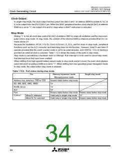
33

 MITSUBISHI [ Mitsubishi Group ]