MT93L16
Preliminary Information
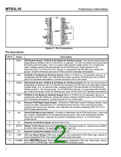
IC
35 IC
ENA1
MD1
1
2
3
4
5
36
34
IC
ENA2
33 MCLK2
NC
32
MD2
Rin
VSS
Sin
31
6
30
VDD2
IC
7
29 VSS2
28 IC
8
MCLK
IC
9
QSOP
27
IC
10
11
12
13
14
15
IC
26 BCLK/C4i
IC
25 F0i
LAW
FORMAT
RESET
NC
24
23
Rout
Sout
22 VDD
NC
21
NC
SCLK
CS 18
16
17
20 DATA1
19 DATA2
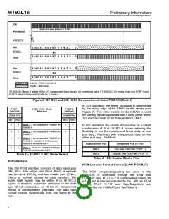
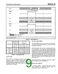
Figure 2 - Pin Connections
Pin Description
Pin #
Name
Description
1
ENA1
SSI Enable Strobe / ST-BUS & GCI Mode for Rin/Sout (Input). This pin has dual functions
depending on whether SSI or ST-BUS/GCI is selected. For SSI, this strobe must be present
for frame synchronization. This is an active high channel enable strobe, 8 or 16 data bits
wide, enabling serial PCM data transfer for on Rin/Sout pins. Strobe period is 125
microseconds. For ST-BUS or GCI, this pin, in conjunction with the MD1 pin, selects the
proper mode for Rin/Sout pins (see ST-BUS and GCI Operation description).
2
3
MD1
ST-BUS & GCI Mode for Rin/Sout (Input). When in ST-BUS or GCI operation, this pin, in
conjunction with the ENA1 pin, will select the proper mode for Rin/Sout pins (see ST-BUS
and GCI Operation description). Connect this pin to Vss in SSI mode.
ENA2
SSI Enable Strobe / ST-BUS & GCI Mode for Sin/Rout (Input).This pin has dual functions
depending on whether SSI or ST-BUS/GCI is selected. For SSI, this is an active high channel
enable strobe, 8 or 16 data bits wide, enabling serial PCM data transfer on Sin/Rout pins.
Strobe period is 125 microseconds. For ST-BUS/GCI, this pin, in conjunction with the MD2
pin, selects the proper mode for Sin/Rout pins (see ST-BUS and GCI Operation description).
4
5
MD2
Rin
ST-BUS & GCI Mode for Sin/Rout (Input).When in ST-BUS or GCI operation, this pin in
conjunction with the ENA2 pin, selects the proper mode for Sin/Rout pins (see ST-BUS and
GCI Operation description). Connect this pin to Vss in SSI mode.
Receive PCM Signal Input (Input). 128 kbit/s to 4096 kbit/s serial PCM input stream. Data
may be in either companded or 2’s complement linear format. This is the Receive Input
channel from the line (or network) side. Data bits are clocked in following SSI, GCI or ST-
BUS timing requirements.
6
Sin
IC
Send PCM Signal Input (Input). 128 kbit/s to 4096 kbit/s serial PCM input stream. Data may
be in either companded or 2’s complement linear format. This is the Send Input channel
(from the microphone). Data bits are clocked in following SSI,GCI or ST-BUS timing
requirements.
7
8
Internal Connection (Input): Must be tied to Vss.
MCLK Master Clock (Input): Nominal 20 MHz Master Clock input (may be asynchronous relative
to 8KHz frame signal.) Tie together with MCLK2 (pin 33).
9,10,11
12
IC
Internal Connection (Input): Must be tied to Vss.
LAW
A/µ Law Select (Input). When low, selects µ−Law companded PCM. When high, selects A-
Law companded PCM. This control is for both serial pcm ports.
13
FORMAT ITU-T/Sign Mag (Input). When low, selects sign-magnitude PCM code. When high, selects
ITU-T (G.711) PCM code. This control is for both serial pcm ports.
2

 MITEL [ MITEL NETWORKS CORPORATION ]