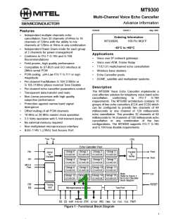
MT9300
Advance Information
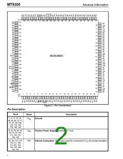
Pin Description (continued)
Pin #
Name
Description
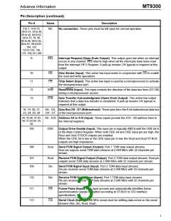
140
MCLK
Master Clock (Input). Nominal 10MHz or 20MHz Master Clock input. May be
connected to an asynchronous (relative to frame signal) clock source.
143
Fsel
Frequency select (Input). This input selects the Master Clock frequency
operation. When Fsel pin is low, nominal 19.2MHz Master Clock input must be
applied. When Fsel pin is high, nominal 9.6MHz Master Clock input must be
applied.
146
147
152
PLLV
PLLV
PLL Ground. Must be connected to V
SS
SS
PLL Power Supply. Must be connected to V
DD
DD
TMS
Test Mode Select (3.3V Input). JTAG signal that controls the state transitions of
the TAP controller. This pin is pulled high by an internal pull-up when not driven.
153
154
TDI
Test Serial Data In (3.3V Input). JTAG serial test instructions and data are shifted
in on this pin. This pin is pulled high by an internal pull-up when not driven.
TDO
Test Serial Data Out (Output). JTAG serial data is output on this pin on the falling
edge of TCK. This pin is held in high impedance state when JTAG scan is not
enabled.
155
156
TCK
Test Clock (3.3V Input). Provides the clock to the JTAG test logic.
TRST
Test Reset (3.3V Input). Asynchronously initializes the JTAG TAP controller by
putting it in the Test-Logic-Reset state. This pin should be pulsed low on power-up
or held low, to ensure that the MT9300 is in the normal functional mode. This pin is
pulled by an internal pull-down when not driven.
158
RESET Device Reset (Schmitt Trigger Input). An active low resets the device and puts
the MT9300 into a low-power stand-by mode.
When the RESET pin is returned to logic high and a clock is applied to the
MCLK pin, the device will automatically execute initialization routines, which
preset all the Control and Status Registers to their default power-up values.
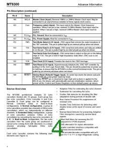
•
•
•
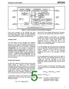
Adaptive Filter for estimating the echo channel
Subtractor for cancelling the echo
Device Overview
Double-Talk detector for disabling the filter
adaptation during periods of double-talk
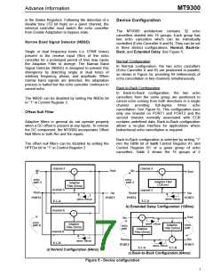
The MT9300 architecture contains 32 echo
cancellers divided into 16 groups. Each group has
two echo cancellers, Echo Canceller A and Echo
Canceller B. Each group can be configured in
•
•
Non-Linear Processor for suppression of
residual echo
Normal,
Extended
Delay
or
Back-to-Back
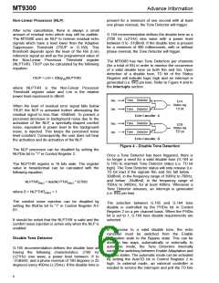
Disable Tone Detectors for detecting valid
disable tones at the input of receive and send
paths
configurations. In Normal configuration, a group of
echo cancellers provides two channels of 64ms echo
cancellation, which run independently on different
channels. In Extended Delay configuration, a group
of echo cancellers achieves 128ms of echo
cancellation by cascading the two echo cancellers (A
& B). In Back-to-Back configuration, the two echo
cancellers from the same group are positioned to
cancel echo coming from both directions in a single
•
•
Narrow-Band Detector for preventing Adaptive
Filter divergence caused by narrow-band
signals
Offset Null filters for removing the DC
component in PCM channels
•
•
12dB attenuator for signal attenuation
channel,
providing
full-duplex
64ms
echo
Parallel controller interface compatible with
Motorola microcontrollers
cancellation.
•
PCM encoder/decoder compatible with µ/A-
Law ITU-T G.711 or Sign-Magnitude coding
Each echo canceller contains the following main
elements (see Figure 3).
4

 MITEL [ MITEL NETWORKS CORPORATION ]