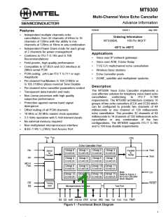
Advance Information
MT9300
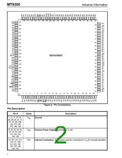
Pin Description (continued)
Pin #
Name
Description
3 to 7, 14 to 16,
28 to 31, 33 to 36,
39 to 42, 60 to 62,
64 to 75, 78, 80,
82 to 86, 88 to 92,
94 to 97, 99 to102,
104, 123,
NC
No connection. These pins must be left open for normal operation.
125 to 132, 136,
137, 150,151,160
9
IRQ
Interrupt Request (Open Drain Output). This output goes low when an interrupt
occurs in any channel. IRQ returns high when all the interrupts have been read
from the Interrupt FIFO Register. A pull-up resistor (1K typical) is required at this
output.
10
11
12
13
DS
CS
Data Strobe (Input). This active low input works in conjunction with CS to enable
the read and write operations.
Chip Select (Input). This active low input is used by a microprocessor to activate
the microprocessor port.
R/W
DTA
Read/Write (Input). This input controls the direction of the data bus lines (D7-D0)
during a microprocessor access.
Data Transfer Acknowledgment (Open Drain Output). This active low output
indicates that a data bus transfer is completed. A pull-up resistor (1K typical) is
required at this output.
18, 19, 20, 21,
23, 24, 25, 26
D0 - D3, Data Bus D0 - D7 (Bidirectional). These pins form the 8-bit bidirectional data bus
D4 - D7 of the microprocessor port.
44, 45,46, 47,49,
50, 51,52,54, 55,
56
A0 - A10 Address A0 to A10 (Input). These inputs provide the A10 - A0 address lines to
the internal registers.
105
ODE
Sout
Output Drive Enable (Input). This input pin is logically AND’d with the ODE bit-6
of the Main Control Register. When both ODE bit and ODE input pin are high, the
Rout and Sout ST-BUS outputs are enabled.
When the ODE bit is low or the ODE input pin is low, the Rout and Sout ST-BUS
outputs are high impedance.
106
Send PCM Signal Output (Output). Port 1 TDM data output streams.
Sout pin outputs serial TDM data streams at 2.048 Mb/s with 32 channels per
stream.
107
109
Rout
Sin
Receive PCM Signal Output (Output). Port 2 TDM data output streams. Rout pin
outputs serial TDM data streams at 2.048 Mb/s with 32 channels per stream.
Send PCM Signal Input (Input). Port 2 TDM data input streams.
Sin pin receives serial TDM data streams at 2.048 Mb/s with 32 channels per
stream.
110
111
Rin
F0i
Receive PCM Signal Input (Input). Port 1 TDM data input streams.
Rin pin receives serial TDM data streams at 2.048 Mb/s with 32 channels per
stream.
Frame Pulse (Input). This input accepts and automatically identifies frame
synchronization signals formatted according to ST-BUS or GCI interface
specifications.
112
C4i
Serial Clock (Input). 4.096 MHz serial clock for shifting data in/out on the serial
streams (Rin, Sin, Rout, Sout).
3

 MITEL [ MITEL NETWORKS CORPORATION ]