Advance Information
MT9160B/61B
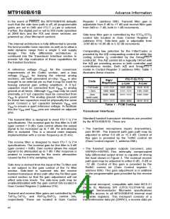
Filter/Codec and Transducer Interface
Serial
Port
Default Bypass
HSPKR +
-8.05 dB or
-2.05 dB
Receive
Filter Gain
0 to -7 dB
(1 dB steps)
Handset
Receiver
(150Ω)
Decoder
2.05dB
PCM
Receiver
Driver
75Ω
HSPKR -
-6 dB
Din
75Ω
Side-tone
-9.96 to
+9. 96 dB
(3.32 dB steps)
-11 dB
M+
M-
Transmit
Transmit Filter
PCM
Transmit Filter
Transmitter
Microphone
Transmit Gain
Encoder
-2.05dB
Gain
Gain
Gain
-0.37 dB or 8.93 dB
0 to +7 dB
0 to +7 dB
(1 dB steps)
8.42 dB
Dout
(1 dB steps)
INTERNAL TO DEVICE
EXTERNAL TO DEVICE
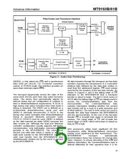
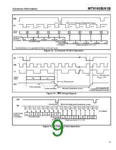
Figure 3 - Audio Gain Partitioning
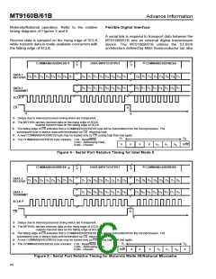
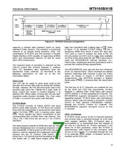
(DATA2), a chip select pin (CS) and a synchronous
data clock pin (SCLK). For D-channel contention
control, in ST-BUS mode, this interface provides an
open-drain interrupt output (IRQ).
All data transfers through the microport are two-byte
transfers requiring the transmission of a Command/
Address byte followed by the data byte written or
read from the addressed register. CS must remain
asserted for the duration of this two-byte transfer. As
shown in Figures 5 and 6 the falling edge of CS
indicates to the MT9160B/61B that a microport
transfer is about to begin. The first 8 clock cycles of
SCLK after the falling edge of CS are always used to
receive the Command/Address byte from the
The microport dynamically senses the state of the
serial clock (SCLK) each time chip select becomes
active. The device then automatically adjusts its
internal timing and pin configuration to conform to
Intel or Motorola/National requirements. If SCLK is
high during chip select activation then Intel mode 0
timing is assumed. The DATA1 pin is defined as a
bi-directional (transmit/receive) serial port and
DATA2 is internally disconnected. If SCLK is low
during chip select activation then Motorola/National
timing is assumed. Motorola processor mode
CPOL=0, CPHA=0 must be used. DATA1 is defined
as the data transmit pin while DATA2 becomes the
data receive pin. Although the dual port Motorola
controller configuration usually supports full-duplex
communication, only half-duplex communication is
possible in the MT9160B/61B. The micro must
discard non-valid data which it clocks in during a
valid write transfer to the MT9160B/61B. During a
valid read transfer from the MT9160B/61B data
simultaneously clocked out by the micro is ignored
by the MT9160B/61B.
microcontroller.
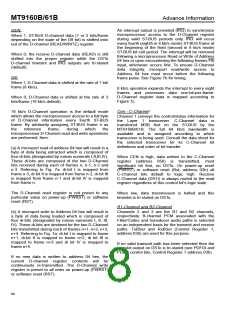
The
Command/Address
byte
contains information detailing whether the second
byte transfer will be a read or a write operation and
at what address. The next 8 clock cycles are used to
transfer the data byte between the MT9160B/61B
and the microcontroller. At the end of the two-byte
transfer CS is brought high again to terminate the
session. The rising edge of CS will tri-state the
output driver of DATA1 which will remain tri-stated as
long as CS is high.
Intel processors utilize least significant bit first
transmission while Motorola/National processors
employ most significant bit first transmission. The
MT9160B/61B
microport
automatically
accommodates these two schemes for normal data
bytes. However, to ensure decoding of the R/W and
address information, the Command/Address byte is
defined differently for Intel operation than it is for
83

 MITEL [ MITEL NETWORKS CORPORATION ]