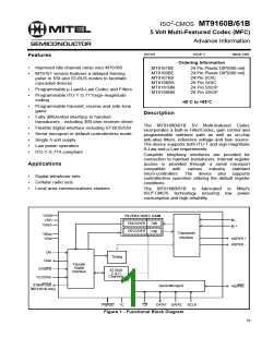
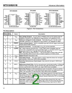
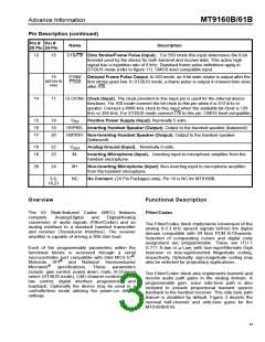
MT9160B/61B
Advance Information
In the event of PWRST, the MT9160B/61B defaults
such that the side-tone path is off, all programmable
gains are set to 0dB and ITU-T µ-Law is selected.
Further, the digital port is set to SSI mode operation
at 2048 kb/s and the FDI and driver sections are
powered up. (See Microport section)
Register 1 (address 00h). Transmit filter gain is
adjustable from 0 dB to +7 dB and receive filter gain
from 0dB to -7 dB, both in 1 dB increments.
Side-tone filter gain is controlled by the STG -STG
0
2
control bits located in Gain Control Register 2
(address 01h). Side-tone gain is adjustable from
-9.96 dB to +9.96 dB in 3.32 dB increments.
The internal architecture is fully differential to provide
the best possible noise rejection as well as to allow a
wide dynamic range from a single 5 volt supply
design. This fully differential architecture is
continued into the Transducer Interface section to
provide full chip realization of these capabilities for
the handset functions.
Companding law selection for the Filter/Codec is
provided by the A/µ companding control bit while the
coding scheme is controlled by the Smag/ITU-T
control bit. The A/µ control bit is logically OR’ed with
the A/µ pin providing access in both controller and
controllerless modes. Both A/µ and Smag/ITU-T
reside in Control Register 2 (address 04h). Table 1
illustrates these choices.
A reference voltage (V ), for the conversion
Ref
requirements of the Codec section, and a bias
voltage (V
), for biasing the internal analog
Bias
sections, are both generated on-chip. V
brought to an external pin so that it may be used for
biasing external gain setting amplifiers. A 0.1µF
is also
ITU-T (G.711)
Sign/
Bias
Code
Magnitude
µ-Law
A-Law
+ Full Scale
+ Zero
1111 1111
1000 0000
0000 0000
1000 0000
1111 1111
0111 1111
1010 1010
1101 0101
0101 0101
capacitor must be connected from V
to analog
Bias
ground at all times. Although V
may only be used
Ref
internally, a 0.1µF capacitor must be connected from
to ground. The analog ground reference point
-Zero
(quiet code)
V
Ref
for these two capacitors must be physically the same
point. Connect a 1µF capacitor between V and
- Full Scale
0111 1111
0000 0000
0010 1010
Bias
Table 1 - PCM Coding
V
to ensure a quiet reference voltage. To facilitate
Ref
this the V
pins.
and V
pins are situated on adjacent
Ref
Bias
Transducer Interfaces
Standard handset transducer interfaces are provided
by the MT9160B/61B. These are:
The transmit filter is designed to meet ITU-T G.714
specifications. The nominal gain for this filter is 0 dB
(gain control = 0 dB). Gain control allows the output
signal to be increased up to 7 dB. An anti-aliasing
filter is included. This is a second order lowpass
implementation with a corner frequency at 25 kHz.
• The handset microphone inputs (transmitter),
pins M+/M-. The transmit path gain path may be
adjusted to either 6.0 dB or 15.3 dB. Control of
this gain is provided by the TxINC control bit
(Gain Control register 1, address 00h).
The receive filter is designed to meet ITU-T G.714
specifications. The nominal gain for this filter is 0 dB
(gain control = 0dB). Gain control allows the output
signal to be attenuated up to 7 dB. Filter response is
peaked to compensate for the sinx/x attenuation
caused by the 8 kHz sampling rate.
• The handset speaker outputs (receiver), pins
HSPKR+/HSPKR-.This internally compensated
fully differential output driver is capable of driving
the load shown in Figure 3. The nominal receive
path gain may be adjusted to either 0 dB, -6 dB or
-12 dB. Control of this gain is provided by the
RxINC control bit (Gain Control register 1,
address 00h). This gain adjustment is in addition
to the programmable gain provided by the receive
filter.
Side-tone is derived from the input of the Tx filter and
is not subject to the gain control of the Tx filter
section. Side-tone is summed into the receive
handset transducer driver path after the Rx filter gain
control section so that Rx gain adjustment will not
affect side-tone levels. The side-tone path may be
enabled/disabled with the gain control bits located in
Gain Control Register 2 (address 01h).
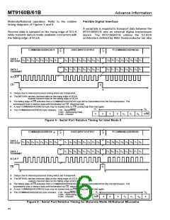
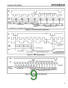
The serial microport, compatible with Intel MCS-51
(mode 0), Motorola SPI (CPOL=0,CPHA=0) and
National Semiconductor Microwire specifications
provides access to all MT9160B/61B internal read
and write registers. This microport consists of a
transmit/receive data pin (DATA1), a receive data pin
Transmit and receive filter gains are controlled by the
TxFG -TxFG
and RxFG -RxFG
control bits,
0
2
0
2
respectively. These are located in Gain Control
82

 MITEL [ MITEL NETWORKS CORPORATION ]