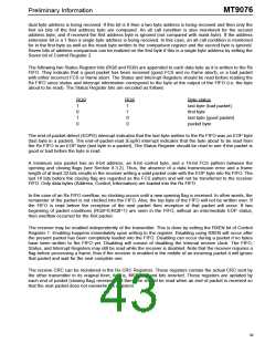
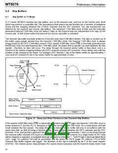
Preliminary Information
MT9076
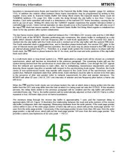
The minimum delay through the receive slip buffer is approximately two channels and the maximum delay is
approximately 60 channels (see Figure 14).
When the C4b and the Exclk clocks are not phase-locked, the rate at which data is being written into the slip
buffer from the PCM 30 side may differ from the rate at which it is being read out onto the ST-BUS. If this
situation persists, the delay limits stated in the previous paragraph will be violated and the slip buffer will
perform a controlled frame slip. That is, the buffer pointers will be automatically adjusted so that a full PCM 30
frame is either repeated or lost. All frame slips occur on PCM 30 frame boundaries.
Two status bits, RSLIP and RSLPD (page03H, address13H) give indication of a slip occurance and direction.
RSLIP changes state in the event of a slip. If RSLPD=0, the slip buffer has overflowed and a frame was lost; if
RSLPD=1, a underflow condition occurred and a frame was repeated. A maskable interrupt SLPI (page 01H,
address 1BH) is also provided.
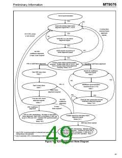
Figure 14 illustrates the relationship between the read and write pointers of the receive slip buffer. Measuring
clockwise from the write pointer, if the read pointer comes within two channels of the write pointer a frame slip
will occur, which will put the read pointer 34 channels from the write pointer. Conversely, if the read pointer
moves more than 60 channels from the write pointer, a slip will occur, which will put the read pointer 28
channels from the write pointer. This provides a worst case hysteresis of 13 channels peak (26 channels peak-
to-peak) or a wander tolerance of 208 UI.
Write
Pointer
Read Pointer
Read Pointer
60 CH
13 CH
2 CH
Wander Tolerance
512 Bit
Elastic
Store
15 CH
47 CH
-13 CH
34 CH
28 CH
Read Pointer
Read Pointer
Figure 14 - Read and Write Pointers in the Slip Buffers
10.0 Framing Algorithm
10.1
Frame Alignment in T1 Mode
In T1 mode, MT9076 will synchronize to DS1 lines formatted with either the D4 or ESF protocol. In either mode
the framer maintains a running 3 bit history of received data for each of the candidate bit positions. Candidate
bit positions whose incoming patterns fail to match the predicted pattern (based on the 3 bit history) are
winnowed out. If, after a 10 bit history has been examined, only one candidate bit position remains within the
framing bit period, the receive side timebase is forced to align to that bit position. If no candidates remain after
a 10 bit history, the process is re-initiated. If multiple candidates exist after a 24 bit history timeout period, the
framer forces the receive side timebase to synchronize to the next incoming valid candidate bit position. In the
event of a reframe, the framer starts searching at the next bit position over. This prevents persistent locking to
a mimic as the controller may initiate a software controlled reframe in the event of locking to a mimic.
Under software control the framing criteria may be tuned (see Framing Mode Select Register, page 1H,
address 10H). Selecting D4 framing invites a further decision whether or not to include a cross check of Fs bits
along with the Ft bits. If Fs bits are checked (by setting control bit CXC high - bit 5 of the Framing Mode Select
43

 MITEL [ MITEL NETWORKS CORPORATION ]