Preliminary Information
MT9076
boundary is measured every frame and reported in the Transmit Slip Buffer Delay register- (page 3H, address
17H). In addition the relative offset between these frame boundaries may be programmed by writing to this
register. Every write to Transmit Elastic Buffer Set Delay Word resets the transmit elastic frame count bit
TxSBMSB (address 17H, page 3H). After a write the delay through the slip buffer is less than 1 frame in
duration. Each write operation will result in a disturbance of the transmit DS1 frame boundary, causing the far
end to go out of sync. Writing BC (hex) into the TxSBDLY register maximizes the wander tolerance before a
controlled slip occurs. Under normal operation no slips should occur in the transmit path. Slips will only occur if
the input C4b clock has excess wander, or the Transmit Elastic Buffer Set Delay Word register is initialized too
close to the slip pointers after system initialization.
The two frame receive elastic buffer is attached between the 1.544 Mbit/s DS1 receive side and the 2.048 Mbit/
s ST-BUS side of the MT9076. Besides performing rate conversion, this elastic buffer is configured as a slip
buffer which absorbs wander and low frequency jitter in multi-trunk applications. The received DS1 data is
clocked into the slip buffer with the Exclk clock and is clocked out of the slip buffer with the system C4b clock.
The Exclk extracted clock is generated from, and is therefore phase-locked with, the receive DS1 data. In the
case of Internal mode (pin BS/LS set low) operation, the Exclk clock may be phase-locked to the C4b clock by
an internal phase locked loop (PLL). Therefore, in a single trunk system the receive data is in phase with the
Exclk clock, the C4b clock is phase locked to the E1.5o clock, and the read and write positions of the slip buffer
track each other.
In a multi-trunk slave or loop-timed system (i.e., PABX application) a single trunk will be chosen as a network
synchronizer, which will function as described in the previous paragraph. The remaining trunks will use the
system timing derived from the synchronizer to clock data out of their slip buffers. Even though the DS1 signals
from the network are synchronous to each other, due to multiplexing, transmission impairments and route
diversity, these signals may jitter or wander with respect to the synchronizing trunk signal. Therefore, the Exclk
clocks of non-synchronized trunks may wander with respect to the Exclk clock of the synchronizer and the
system bus. Network standards state that, within limits, trunk interfaces must be able to receive error-free data
in the presence of jitter and wander (refer to network requirements for jitter and wander tolerance). The
MT9076 will allow 92 usec (140 UI, DS1 unit intervals) of wander and low frequency jitter before a frame slip
will occur.
When the C4b and the Exclk clocks are not phase-locked, the rate at which data is being written into the slip
buffer from the DS1 side may differ from the rate at which it is being read out onto the ST-BUS. If this situation
persists, the delay limits stated in the previous paragraph will be violated and the slip buffer will perform a
controlled frame slip. That is, the buffer pointers will be automatically adjusted so that a full DS1 frame is either
repeated or lost. All frame slips occur on frame boundaries.
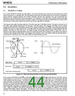
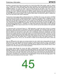
The minimum delay through the receive slip buffer is approximately 1 usec and the maximum delay is
approximately 249 uS. Figure 14 illustrates the relationship between the read and write pointers of the receive
slip buffer (contiguous time slot mapping). Measuring clockwise from the write pointer, if the read page pointer
comes within 8 usec of the write page pointer a frame slip will occur, which will put the read page pointer 157
usec from the write page pointer. Conversely, if the read page pointer moves more than 249 usec from the write
page pointer, a slip will occur, which will put the read page pointer 124 usec from the write page pointer. This
provides a worst case hysteresis of 92 usec peak = 142 U.I.
41

 MITEL [ MITEL NETWORKS CORPORATION ]