MT9076
Preliminary Information
9.0 Slip Buffers
9.1
Slip Buffer in T1 Mode
In T1 mode, MT9076 contains two slip buffers, one on the transmit side, and one on the receive side. Both
sides may perform a controlled slip. The mechanisms that govern the slip function are a function of backplane
timing and the mapping between the ST-BUS channels and the DS1 channels. The slip mechanisms are
different for the transmit and receive slip buffers. The extracted 1.544 Mhz clock (Exclk) and the internally
generated transmit 1.544 Mhz clock are distinct. Slips on the transmit side are independent from slips on the
receive side. In IMA mode neither the transmit nor receive slip buffer is activated.
The transmit slip buffer has data written to it from the near end 2.048 Mb/s stream. The data is clocked out of
the buffer using signals derived from the transmit 1.544 Mhz clock. The transmit 1.544 Mhz clock is always
phase locked to the DSTi 2.048 Mb/s stream. If the system 4.096 Mhz clock (C4b) is internally generated (pin
BS/LS low), then it is hard locked to the 1.544 Mhz clock. No phase drift or wander can exist between the two
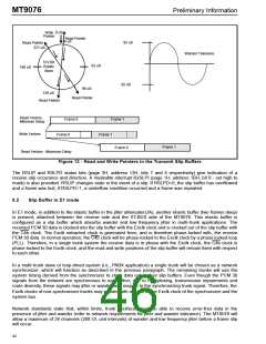
signals - therefore no slips will occur. The delay through the transmit elastic buffer is then fixed, and is a
function of the relative mapping between the DSTi channels and the DS1 timeslots. These delays vary with the
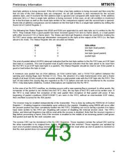
position of the channel in the frame. For example, DS1 timeslot 1 sits in the elastic buffer for approximately 1
usec and DS1 timeslot 24 sits in the elastic buffer for approximately 32 usec.
0 uS
Write
Pointer
Read Pointer
4 uS
92 uS
Read Pointer
221 uS
Wander Tolerance
512 Bit
Elastic
Store
62 uS
188 uS
92 uS
96 uS
Read Pointer
129 uS
Read Pointer
Read Vectors
Minimum Delay
Frame 0
Frame 1
Write Vectors
Frame 0
Frame 1
Frame 1
Frame 0
Read Vectors - Maximum Delay
Figure 12 - Read and Write Pointers in the Transmit Slip Buffers
If the system 4.096 Mhz clock (C4b) is externally generated (pin BS/LS high), the transmit 1.544 Mhz clock is
phase locked to it, but the PLL is designed to filter jitter present in the C4b clock. As a result phase drift will
result between the two signals. The delay through the transmit elastic buffer will vary in accordance with the
input clock drift, as well as being a function of the relative mapping between the DSTi channels and the DS1
timeslots. If the read pointers approach the write pointers (to within approximately 1 usec) or the delay through
the transmit buffer exceeds 218 usecs a controlled slip will occur. The contents of a single frame of DS1 data
will be skipped or repeated; a maskable interrupt (masked by setting bit 1 - TxSLPI high in Interrupt Mask Word
Zero - page 1H, address 1bH) will be generated, and the status bit TSLIP (page 3H, address 17H) of MSB
Transmit Slip Buffer register will toggle. The direction of the slip is indicated by bit 6 of the same register
(TSLPD). The relative phase delay between the system frame boundary and the transmit elastic frame read
40

 MITEL [ MITEL NETWORKS CORPORATION ]