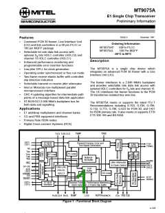
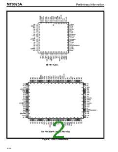
Preliminary Information
MT9075A
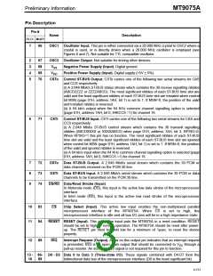
Pin Description (continued)
Pin #
Name
Description
PLCC MQFP
45
33
C4b
4.096 MHz System Clock (Input/Output). C4b is the clock for the ST-BUS sections and
transmit serial PCM data of the MT9075A. In the free-run (BL/FR=0) or line synchronous
mode (BL/FR=1 and BS/LS=0) this signal is an output, while in the system bus
synchronous mode (BS/LS=1) this signal is an input clock.
46
34
F0b
Frame Pulse (Input/Output). This is the ST-BUS or GCI frame synchronization
signal, which delimits the 32 channel frame of CSTi, CSTo, DSTi, DSTo and the
PCM30 link. In the free-run (BL/FR=0) or loop synchronous mode (BL/FR=1 and BS/
LS=0) this signal is an output, while in the Bus Synchronous mode (BL/FR=1 and BS/
LS=0) this signal is an input. The GCI/ST-BUS selection is made under software control.
Page 02H, address 13H, bit 0, GCI/ST=1 selects GCI frame pulse; GCI/ST=0 selects ST-
BUS.
47
35
RxFP/ Receive Frame Pulse/Receive CCS Clock (Output). An 8kHz pulse signal, which is
Rx64KCK low for one extracted clock period. This signal is synchronized to the receive PCM 30
basic frame boundary.
When 64KCCS (page 01H, address 1AH, bit 0) is set to 1, this pin outputs a 64 kHz clock
derived by dividing down the extracted 2.048 MHz clock. This clock is used to clock CCS
data out of pin CSTo in the CCS mode.
48
49
50
51
36
37
38
39
IC
Internal Connection. Must be left open for normal operation.
Negative Power Supply (Input). Digital ground.
V
SS
DD
V
Positive Power Supply (Input). Digital supply (+5V ± 5%).
VDD
Transmit Analog Power Supply (Input). Analog supply for the LIU transmitter (+5V ±
ATx
5%).
52
53
40
41
TTIP
Transmit TIP and RING (Outputs). Differential outputs for the transmit line signal - must
TRING be transformer coupled (See Figure 4).
54
55
56
57
58
59
60
42
43
44
45
46
47
48
GND
Transmit Analog Ground (Input). Analog ground for the LIU transmitter.
IEEE 1149.1 Test Data Input. If not used, this pin should be pulled high.
IEEE 1149.1 Test Data Output. If not used, this pin should be left unconnected.
IEEE 1149.1 Test Mode Selection (Input). If not used, this pin should be pulled high.
IEEE 1149.1 Test Clock Signal (Input). If not used, this pin should be pulled high.
IEEE 1149.1 Reset Signal (Input). If not used, this pin should be held low.
ATx
Tdi
Tdo
Tms
Tclk
Trst
TAIS
Transmit Alarm Indication Signal (Input). An active low on this input causes the
MT9075A to transmit an AIS (all ones signal) on TTIP and TRING pins. TAIS should be
set to high for normal data transmission.
61
57
LOS
Loss of Signal or Synchronization (Output). When high, and LOS/LOF (page 02H
address 13H bit 2) is zero, this signal indicates that the receive portion of the MT9075A is
either not detecting an incoming signal (bit LLOS on page 03H address 18H is one) or is
detecting a loss of basic frame alignment condition (bit SYNC on page 03H address 10H
is one). If LOS/LOF=1, a high on this pin indicates a loss of signal condition.
62
63
58
59
60
IC
NC
IC
Internal Connection. Tie to V (Ground) for normal operation.
SS
No Connection. Leave open for normal operation.
Internal Connection. Tie to V (Ground) for normal operation.
SS
4-133

 MITEL [ MITEL NETWORKS CORPORATION ]