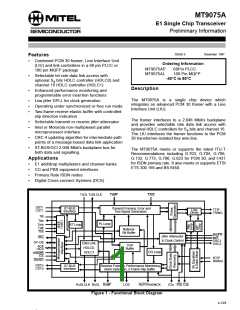
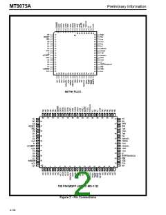
MT9075A
Preliminary Information
Pin Description (continued)
Pin #
Name
Description
PLCC MQFP
17
18
19
90
91
VSS
IC
Negative Power Supply (Input). Digital ground.
Internal Connection. Tie to V (Ground) for normal operation.
SS
92 INT/MOT Intel/Motorola Mode Selection (Input). A high on this pin configures the processor
interface for the Intel parallel non-multiplexed bus type. A low configures the processor
interface for the Motorola parallel non-multiplexed type.
20
93
VDD
Positive Power Supply (Input). Digital supply (+5V ± 5%).
21 - 94-
D4 - D7 Data 4 to Data 7 (Three-state I/O). These signals combined with D0-D3 form the
24
97
bidirectional data bus of the microprocessor interface (D7 is the most significant bit).
25
98
R/W/WR Read/Write/Write Strobe (Input).
In Motorola mode (R/W), this input controls the direction of the data bus D[0:7] during
a microprocessor access. When R/W is high, the parallel processor is reading data
from the MT9075A. When low, the microprocessor is writing data to the MT9075A.
For Intel mode (WR), this active low write strobe configures the data bus lines as
output.
26 - 99,
30 8-11
AC0 - Address/Control 0 to 4 (Inputs). Address and control inputs for the microprocessor
interface. AC0 is the least significant input.
AC4
31
12 GNDARx Receive Analog Ground (Input). Analog ground for the LIU receiver.
32
33
13
14
RTIP
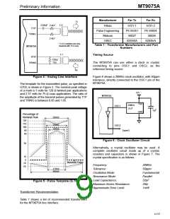
Receive TIP and RING (Inputs). Differential inputs for the receive line signal - must be
RRING transformer coupled (See Figure 4).
34
35
36
37
38
39
15 VDDARx Receive Analog Power Supply (Input). Analog supply for the LIU receiver (+5V ± 5%).
16
17
18
19
VDD
VSS
IC
Positive Power Supply (Input). Digital supply (+5V ± 5%).
Negative Power Supply (Input). Digital ground.
Internal Connection. Must be left open for normal operation.
Internal Connection. Must be left open for normal operation.
IC
20 RxDLCLK Receive Data Link Clock (Output). A gapped clock signal derived from a 2.048 Mbit/s
clock, available for an external device to clock in RxDL data (at 4, 8, 12, 16 or 20 kHz) on
the rising edge.
40
41
21
RxDL Receive Data Link (Output). A 2.048 Mbit/s data stream containing received line data
after HDB3 decoding. This data is clocked out with the rising edge of E2o.
22
TxMF Transmit Multiframe Boundary (Input). An active low input used to set the transmit
multiframe boundary (CAS or CRC multiframe). The MT9075A will generate its own
multiframe if this pin is held high. This input is usually pulled high for most applications.
42
23
RxMF Receive Multiframe Boundary (Output). An output pulse delimiting the received
multiframe boundary. The next frame output on the data stream (DSTo) is basic frame
zero on the PCM 30 link. This receive multiframe signal can be related to either the
receive CRC multiframe (page 01H, address 10H, bit 6, MFSEL=1) or the receive
signalling multiframe (MFSEL=0).
43
44
24
32
BS/LS System Bus Synchronous/Line Synchronous Selection (Input). If high, C4b and F0b
will be inputs; if low, C4b and F0b will be outputs.
E2o
2.048 MHz Extracted Clock (Output). The clock extracted from the received signal
and used internally to clock in data received on RTIP and RRING.
4-132

 MITEL [ MITEL NETWORKS CORPORATION ]