Preliminary Information
MT9075A
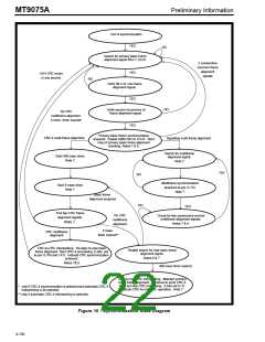
Notes for Synchronization State Diagram
(Figure 10)
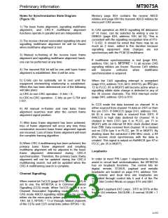
Memory page 05H contains the receive ABCD
nibbles and page 06H the transmit ABCD nibbles for
micro-port CAS access.
1) The basic frame alignment, signalling multiframe
alignment, and CRC-4 multiframe alignment
functions operate in parallel and are independent.
In CAS operation an ABCD signalling bit debounce
of 14 msec. can be selected by writing a one to
DBNCE (page 02H, address 10H, bit 0)). This is
consistent with the signalling recognition time of ITU-
T Q.422. It should be noted that there may be as
much as 2 msec. added to this duration because
signalling equipment state changes are not
synchronous with the PCM 30 multiframe.
2) The receive channel associated signalling bits and
signalling multiframe alignment bit will be frozen
when multiframe alignment is lost.
3) Manual re-framing of the receive basic frame
alignment and signalling multiframe alignment functi-
If multiframe synchronization is lost (page 03H,
address 10H, bit 6, MFSYNC = 1) all receive CAS
signalling nibbles are frozen. Receive CAS nibbles
ons can be performed at any time.
4) The transmit RAI bit will be one until basic frame
alignment is established, then it will be zero.
will
become
unfrozen
when
multiframe
synchronization is acquired.
5) E-bits can be optionally set to zero until the
equipment interworking relationship is established.
When this has been determined one of the following
will take place:
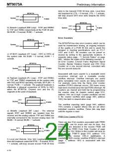
When the CAS signalling interrupt is unmasked
(page 01H, address 1CH, bit 0, SIGI=0), pin IRQ (pin
12 in PLCC, 85 in MQFP) will become active when a
signalling nibble state change is detected in any of
the 30 receive channels. The SIGI interrupt vector
(page 04H, address 12H) is 01H.
a) CRC-to-non-CRC operation - E-bits = 0,
b) CRC-to-CRC operation - E-bits as per G.704 and
I.431.
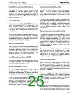
In CCS mode the data transmit on channel 16 is
either sourced from channel 16 data on DSTi or from
the pin CSTi. If 64KCCS (page 01H, address 1AH,
bit 0) is zero the data is sourced from DSTi. If
64KCCS is high data destined for channel 16 is
clocked in from CSTi (pin 6 in PLCC, pin 71 in
MQFP) with an internal 64 KHz clock divided down
from C4b. Data received from channel 16 is clocked
out on CSTo (pin 5 in PLCC, pin 70 in MQFP). By
dividing down the extracted 2.048 MHz clock, a 64
kHz receive clock synchronous with the data is
created. This signal is output on Rx64KCK (pin 47 in
PLCC, pin 35 in MQFP).
6) All manual re-frames and new basic frame
alignment searches start after the current frame
alignment signal position.
7) After basic frame alignment has been achieved,
loss of frame alignment will occur any time three
consecutive incorrect basic frame alignment signals
are received. Loss of basic frame alignment will reset
the complete framing algorithm.
8) When CRC-4 multiframing has been achieved, the
primary basic frame alignment and resulting
multiframe alignment will be adjusted to the basic
frame alignment determined during CRC-4
synchronization. Therefore, the primary basic frame
alignment will not be updated during the CRC-4
multiframing search, but will be updated when the
CRC-4 multiframing search is complete.
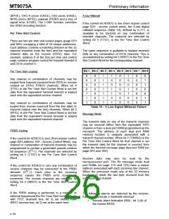
Loopbacks
In order to meet PRI Layer 1 requirements and to
assist in circuit fault sectionalization, the MT9075A
has six loopback functions. The control bits for
digital, remote, ST-BUS, payload and metallic
loopbacks are located on page 01H, address 15H.
The remote and local time slot loopbacks are
controlled through control bits 5 and 4 of the Per
Time Slot Control Words on pages 07H and 08H.
Channel Signalling
When control bit TxCCS (page 01H, address 1AH) is
set to one, the MT9075A is in Common Channel
Signalling (CCS) mode. When TxCCS is low it is in
Channel Associated Signalling mode (CAS). The
CAS mode ABCD signalling nibbles can be passed
either via the micro-ports (when page 01H, address
1AH, bit 3, RPSIG = 1) or through related channels
of the CSTo and CSTi serial links (when RPSIG = 0).
a) Digital Loopback (DG Loop) - DSTi to DSTo at the
framer LIU interface. Bit DLBK = 0 normal; DLBK = 1
activate.
4-151

 MITEL [ MITEL NETWORKS CORPORATION ]