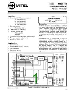
Advance Information
CMOS MT90732
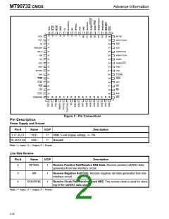
Microprocessor Interface
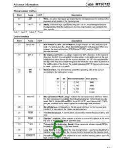
Pin #
Name
I/O/P
Description
47
WR
I
Write. An active low signal generated by the microprocessor for writing to the
registers which reside in the memory map.
48
RDY
O
Ready. An active high signal indicating an E2/E3F acknowledgment to the
microprocessor that the addressed memory map location can complete the
data transfer.
Note: I = Input; O = Output; P = Power
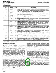
Control Interface
Pin #
Name
I/O/P
Description
13
NRZLINE
I
Non-Return to Zero Line Selection. A high enables an NRZ line input (RP
and TP), and causes the HDB3 decoder/encoder to be bypassed. When low
enables the dual rail interface (RP/RN and TP/TN) and the HDB3
decoder/encoder.
14
BIP-4
I
I
Bit Interleaved Parity - 4. A high enables the BIP-4 function. In the transmit
direction, the BIP-4 is calculated for data nibbles only, and is sent as the last
nibble in the frame format. In the receive direction, the BIP-4 is calculated for
the data bits only and compared against the received value which is present in
the last four bits of the frame. An output indication (BIP-4E) occurs when one
or more columns do not match.
16
15
M1
M0
Mode Control. The two controls select the operating rate of the E2/E3F
according to the table given below.
M1
M0
Recommendation Rate (kbit/s)
0
0
1
1
0
1
0
1
G.745
G.742
G.753
G.751
8448
8448
34368
34368
19
MICRO
I
Microprocessor Mode. A high enables the microprocessor interface. When
the microprocessor is enabled, the following hardware control leads are dis-
abled. BIP-4, Mode (M0 and M1), Serial I/O (SER), and transmit AIS (TAIS).
Bits are provided in the memory map for controlling these functions.
20
21
22
23
24
26
SER
TLBK
PLBK
TAIS
LPT
I
I
I
I
I
I
Serial Interface. A high selects the bit-serial interface for the terminal side
interface. A low selects the nibble-parallel interface.
Terminal Loopback. A low enables a transmit to receive loopback at the line
side.
Payload Loopback. A low enables a receive to transmit loopback at the termi-
nal side in the serial mode of operation only.
Transmit Alarm Indication Signal. A low causes an all ones signal (AIS) to
be sent in place of a G.7XX frame format.
Loop Timing. A low enables the loop timing feature. Loop timing disables the
transmit clock and enables the receive clock to be used as the transmit clock.
FORCEFE
Force Framing Error. The errored bit is sent into the framing pattern upon the
high-to-low transition of this pin.
5-19

 MITEL [ MITEL NETWORKS CORPORATION ]