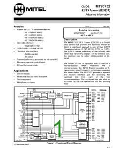
MT90732 CMOS
Advance Information
10
ROC
ROF
BIP-4E
XNC/TCOUT
XNF
60
59
58
57
56
55
54
53
52
51
50
49
48
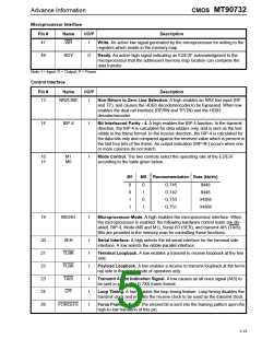
47
46
45
11
12
13
14
15
16
17
18
19
20
21
22
23
24
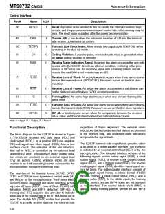
FE
NRZLINE
BIP-4
M0
XCK
XNIB0/XSD
XNIB1/TCIN
XNIB2
XNIB3/XSF
GND
M1
VDD
GND
VDD
MICRO
SER
TLCINV
DAIS
TLBK
PLBK
TAIS
RDY
WR
RD
LPT
ALE
TLOC
FORCEFE
25
26
SEL
44
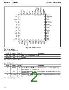
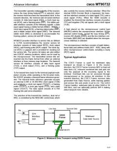
Figure 2 - Pin Connections
Pin Description
Power Supply and Ground
Pin #
Name
I/O/P
Description
1,17,35,51
VDD
GND
P
P
VDD. 5-volt supply voltage, +/- 5%
18,34,52,68
Ground.
Note: I = Input; O = Output; P = Power
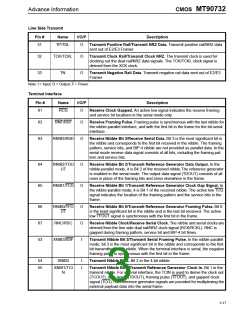
Line Side Receive
Pin #
Name
I/O/P
Description
2
RP/RDL
I
Receive Positive Rail/Receive NRZ Data. Receive positive rail/NRZ data
generated from line interface circuit.
3
4
RN
I
I
Receive Negative Rail Data. Receive negative rail data generated from line
interface circuit.
RCK/RCKL
Receive Clock Rail/Receive Clock NRZ. The receive clock is used for clock-
ing in the rail/NRZ data signals.
Note: I = Input; O = Output; P = Power
5-16

 MITEL [ MITEL NETWORKS CORPORATION ]