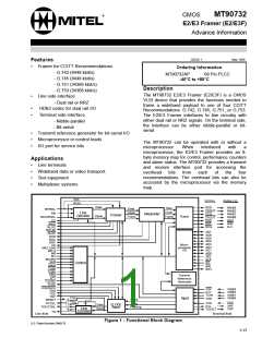
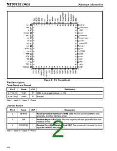
Advance Information
CMOS MT90732
Line Side Transmit
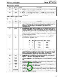
Pin #
Name
I/O/P
Description
31
TP/TDL
O
Transmit Positive Rail/Transmit NRZ Data. Transmit positive rail/NRZ data
sent out of E2/E3 Framer.
32
33
TCK/TCKL
TN
O
O
Transmit Clock Rail/Transmit Clock NRZ. The transmit clock is used for
clocking out the dual rail/NRZ data signals. The TCK/TCKL clock signal is
derived from the XCK clock.
Transmit Negative Rail Data. Transmit negative rail data sent out of E2/E3
Framer.
Note: I = Input; O = Output; P = Power
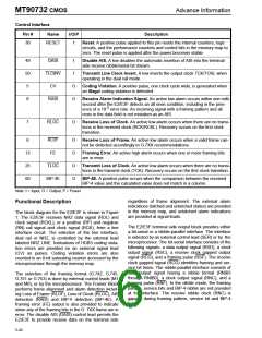
Terminal Interface
Pin #
Name
I/O/P
Description
61
RCG
O
Receive Clock Gapped. An active low signal indicates the receive framing
and service bit locations in the serial mode only.
62
63
RNF/RSF
O
O
Receive Framing Pulse. Framing pulse is synchronous with the last nibble for
the nibble-parallel interface, and with the first bit in the frame for the bit-serial
interface.
RNIB3/RSD
Receive Nibble Bit 3/Receive Serial Data. Bit 3 is the most significant bit in
the nibble and corresponds to the first bit received in the nibble. The framing
pattern, service bits, and BIP-4 nibble are not provided as parallel data. In the
serial mode receive data signal consists of all bits, including the framing pat-
tern and service bits.
64
65
RNIB2/TDO
UT
O
O
Receive Nibble Bit 2/Transmit Reference Generator Data Output. In the
nibble-parallel mode, it is Bit 2 of the received nibble.The reference generator
is enabled in the serial mode. The output data signal (TDOUT) consists of all
ones in place of the framing bits and zeros elsewhere in the frame.
RNIB1/TCG
Receive Nibble Bit 1/Transmit Reference Generator Clock Gap Signal. In
the nibble-parallel mode, it is Bit 1 of the received nibble. The active low TCG
signal indicates the location of the framing pattern and the service bits in the
frame.
66
67
53
RNIB0/TFO
UT
O
O
I
Receive Nibble Bit 0/Transmit Reference Generator Framing Pulse. Bit 0
is the least significant bit in the nibble and is the last bit received. The active
low TFOUT signal is synchronous with the first bit in the frame.
RNC/RSC
Receive Nibble Clock/Receive Serial Clock. The nibble and serial clocks are
derived from the line side dual rail/NRZ clock signal (RCK/RCKL). RNC is
gapped during framing pattern, service bit and BIP-4 bit times.
XNIB3/XSF
Transmit Nibble Bit 3/Transmit Serial Framing Pulse. In the nibble-parallel
mode, bit 3 is the most significant bit in the nibble and corresponds to the first
bit transmitted in the nibble. When the terminal interface is serial, the negative
framing pulse is synchronous with the first bit in the frame.
54
55
XNIB2
I
I
Transmit Nibble Bit 2. Bit 2 in the 4-bit nibble.
XNIB1/TCI
N
Transmit Nibble Bit 1/Transmit Reference Generator Clock In. Bit 1 in the
transmit nibble. For a serial interface, the TCIN is used to derive the clock out
(TCOUT), data signal (TDOUT), framing pulse (TFOUT), and gapped clock
signal (TCG).The reference generator signals are provided for multiplexing the
external payload data into the serial frame.
5-17

 MITEL [ MITEL NETWORKS CORPORATION ]