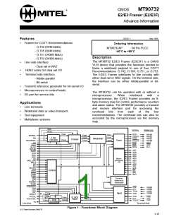
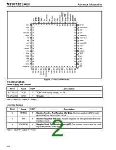
MT90732 CMOS
Advance Information
Terminal Interface
Pin #
Name
I/O/P
Description
56
XNIB0/XSD
I
Transmit Nibble Bit 0/Transmit Serial Data. In the nibble-parallel mode, bit 0
is the least significant bit in the nibble. For a serial interface, the input must
consist of all the bits in the frame.
57
XCK
XNF
I
Transmit Clock. For the terminal side nibble-parallel interface, the XCK is
used for all transmit timing functions, including deriving the nibble output clock
(XNC) and framing pulse (XNF).For the serial interface, this clock may be
derived from the transmit reference generator clock output (TCOUT).
58
59
O
O
Transmit Nibble Framing Pulse. The XNF and clock signal (XNC) are pro-
vided for multiplexing nibble data into the E2/E3 Framer from external circuitry.
The negative framing pulse identifies the first bit in the frame.
XNC/TCOU
T
Transmit Nibble Clock/Transmit Reference Generator Clock Out. The
XNC is derived from the transmit clock (XCK) and is used as a time base for
clocking data out of the external multiplexer and into the E2/E3 Framer. XNC is
gapped during the framing pattern, service bit and BIP-4 bit times. TCOUT is
derived from the input clock (TCIN), and has the same duty cycle.
Note: I = Input; O = Output; P = Power
Service Bit Interface
Pin #
Name
I/O/P
Description
9
ROD
O
Receive Service Data Bits. These service bits are clocked out of E2/E3
Framer on positive transitions of clock signal (ROC).
10
11
27
28
29
ROC
ROF
TOD
TOC
TOF
O
O
I
Receive Service Bits Clock. A gapped clock that clocks out the service bits.
The clock is active only for clocking out the receive service data bits(ROD).
Receive Service Bits Framing Pulse. A positive framing pulse that is syn-
chronous with the first bit in the frame.
Transmit Service Data Bits. The service bits are clocked into E2/E3 Framer
on positive transitions of clock signal (TOC).
O
O
Transmit Service Bits Clock. A gapped clock that clocks in the service bits.
The clock is active only for clocking in the transmit service data bits (TOD).
Transmit Service Bits Framing Pulse. A positive framing pulse that is syn-
chronous with the first bit in the frame.
Note: I = Input; O = Output; P = Power
Microprocessor Interface
Pin #
Name
I/O/P
Description
36-43
AD(7-0)
I/O Address/Data Bus. These leads constitute the time-multiplexed address and
data bus for accessing the registers which reside in the E2/E3F.
44
45
SEL
ALE
I
I
Select. A low enables the microprocessor to access the E2/E3F memory map
for control, status, and alarm information.
Address Latch Enable. An active high signal generated by the microproces-
sor. Used by the microprocessor to hold an address stable during a read/write
bus cycle.
46
RD
I
Read. An active low signal generated by the microprocessor for reading the
registers which reside in the memory map.
5-18

 MITEL [ MITEL NETWORKS CORPORATION ]