MT9041B
Advance Information
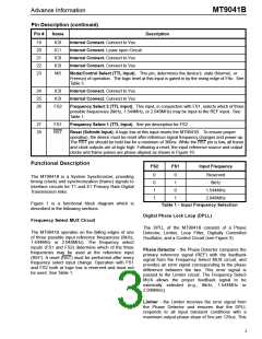
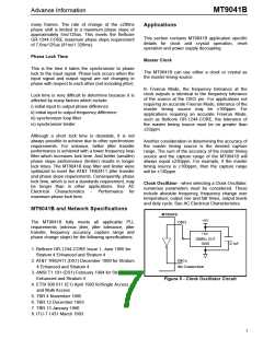
REF Reference
DPLL Reference
to
Output Interface Circuit
Phase
Detector
Digitally
Controlled
Oscillator
Limiter
Loop Filter
Control
Circuit
Feedback Signal
from
Frequency Select MUX
Figure 3 - DPLL Block Diagram
is well within the maximum phase slope of 7.6ns per
125us or 81ns per 1.326ms specified by Bellcore
GR-1244-CORE Stratum 4E.
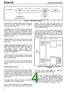
outputs. The C8o, C4o and C2o clocks are
generated by simply dividing the C16o clock by two,
four and eight respectively. These outputs have a
nominal 50% duty cycle.
Loop Filter - the Loop Filter is similar to a first order
low pass filter with a 1.9 Hz cutoff frequency for all
three reference frequency selections (8kHz,
1.544MHz or 2.048MHz). This filter ensures that the
jitter transfer requirements in ETS 300 011 and AT&T
TR62411 are met.
The T1 Divider Circuit uses the 12.384MHz signal to
generate two clock outputs. C1.5o and C3o are
generated by dividing the internal C12 clock by four
and eight respectively. These outputs have a nominal
50% duty cycle.
Control Circuit - the Control Circuit sets the mode
of the DPLL. The two possible modes are Normal
and Freerun.
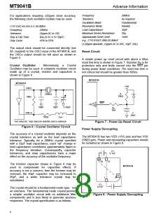
C1.5o
T1 Divider
12MHz
Tapped
Delay
Line
Digitally Controlled Oscillator (DCO) - the DCO
C3o
receives the limited and filtered signal from the Loop
FIlter, and based on its value, generates
a
corresponding digital output signal. The
synchronization method of the DCO is dependent on
the state of the MT9041B.
From
DPLL
In Normal Mode, the DCO provides an output signal
which is frequency and phase locked to the selected
input reference signal.
C2o
C4o
C8o
C16o
F0o
F8o
E1 Divider
16MHz
Tapped
Delay
Line
In Freerun Mode, the DCO is free running with an
accuracy equal to the accuracy of the OSCi 20MHz
source.
F16o
Figure 4 - Output Interface Circuit Block
Diagram
Output Interface Circuit
The output of the DCO (DPLL) is used by the Output
Interface Circuit to provide the output signals shown
in Figure 4. The Output Interface Circuit uses two
Tapped Delay Lines followed by a T1 Divider Circuit
and an E1 Divider Circuit to generate the required
output signals.
The frame pulse outputs (F0o, F8o, F16o) are
generated directly from the C16 clock.
The T1 and E1 signals are generated from a
common DPLL signal. Consequently, the clock
outputs C1.5o, C3o, C2o, C4o, C8o, C16o, F0o and
F16o are locked to one another for all operating
states, and are also locked to the selected input
reference in Normal Mode. See Figures 11 and 12.
Two tapped delay lines are used to generate a
16.384MHz and a 12.352MHz signals.
The E1 Divider Circuit uses the 16.384MHz signal to
generate four clock outputs and three frame pulse
4

 MITEL [ MITEL NETWORKS CORPORATION ]