MT8952B ISO-CMOS
architecture, particularly MITEL’s Digital Network
Interface Circuit (DNIC - MT8972). The data/packets
are shifted in/out serially in ST-BUS format using the
timing signals F0i and C2i/C4i. In addition to framing
the data, the Protocol Controller reserves one
channel (channel-1) on the ST-BUS for carrying
control information (C-channel) and this timeslot can
not be used for the packetized data. While the
Protocol Controller is in the Internal Timing Mode,
the clock input CKi can be either at the bit rate or at
2 bit rate depending on the BRCK bit in the Timing
Control Register as shown in Table 2.
and asynchronous and have effect only after the
current bit in the packet is transmitted/received.
Although the protocol controller provides the
packetized data on a limited number of channels on
the ST-BUS while operating in the Internal Timing
Mode, it can packetize the data on any or all the
channels of the ST-BUS if it is operated in the
External Timing Mode with appropriate enable
signals on TxCEN and RxCEN.
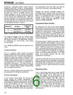
Transparent Data Transfer
Output Data
BRCK Bit
CKi Input
By setting the IFTF bits in the Control Register
appropriately, the protocol functions can be disabled.
This provides a bidirectional access to the serial port
through the microprocessor interface, with 19 byte
deep FIFO in each direction. The transparent data
transfer facility functions in bytewide format and is
available in both timing modes except when the
timing control bits are set for one bit/frame during the
Internal Timing Mode.
Rate
0
1
4.096 MHz/C4i
2.048 MHz/C2i
2.048 Mbps
2.048 Mbps
Table 2. Output Bit Rate In Internal Timing Mode
The Protocol Controller uses the ST-BUS timing
signals F0i and C2iC/ 4i, and enables the transmitter
and receiver sections in the appropriate timeslots
as determined by TC0-TC3 bits in the Timing
Control Register.
The transmit data is shifted out serially on CDSTo
and the operation being bytewide, only the least
significant bits of each byte loaded are transmitted, if
the timing control bits are set to select 2, 6 or 7 bits/
frame. When the transmit FIFO is empty, the last
byte or the portion the last byte, written to the FIFO
is transmitted repeatedly. Similarly the serial data on
CDSTi is shifted in and converted to bytewide
format. In case the timeslot selected is 2, 6 or 7 bits/
frame, the reception involves only the most
significant bits of each byte.
The TxCEN and RxCEN inputs are ignored in this
mode.
C-Channel Interface
This is a separate control channel (C-channel)
interface relevant only in the Internal Timing Mode.
The data stored in the C-Channel Control Register is
shifted out during the channel-1 timeslot of the
outgoing ST-BUS (CDSTo) and the C1EN bit in the
Timing Control Register enables the transmission.
The transmission of C-Channel is independent of
packet/data transmission. The data received on
channel-1 of the incoming ST-BUS (CDSTi) is shifted
into the C-Channel Status Register independently
and it is updated continuously.
It should be noted that none of the protocol related
status or interrupt bits are applicable in transparent
data transfer state. However, the FIFO related status
and interrupt bits are pertinent and carry the same
meaning as they do while performing the protocol
functions.
Watchdog Timer
Both the C-channel registers are accessible by the
accompanying CPU through the parallel port.
This is a fixed eleven stage binary counter with F0i
as the input and WD as the output from the last
stage. This counter can be reset either by the
external input (RST) or by writing XXX0 1010 to the
Watchdog Timer Register. The WD output is
normally HIGH and if the Watchdog Timer Register
External Timing Mode
In the External Timing Mode, the transmit and
receive sections are enabled independently by
TxCEN and RxCEN control inputs and the formatted
data packets are shifted in/out serially at a rate equal
to the clock frequency on CKi. The output is
transmitted on the rising edge and the receiver
samples the input on the falling edge of the clock.
The TxCEN and RxCEN controls are independent
10
is not written within 2 cycles of F0i input after it is
10
reset, the WD output will go LOW for a period of 2
cycles of F0i.
Even though the F0i input is not
required for formatting data in the External Timing
Mode, it is necessary for the operation of the
watchdog timer.
3-66

 MITEL [ MITEL NETWORKS CORPORATION ]