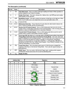
ISO-CMOS MT8952B
Order of Bit Transmission/Reception
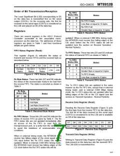
Rx FIFO
Status Bits
Status
The Least Significant Bit (LSB) corresponding to D0
on the data bus is transmitted first on the serial
output (CDSTo). On the receiving side, the first bit
received on the serial input (CDSTi) is considered as
the LSB and placed on D0 of the data bus.
D5
0
D4
0
Rx FIFO Empty
0
1
Less than or equal to 14 bytes
Rx FIFO Full
1
0
1
1
Greater than or equal to 15 bytes
Registers
Table 4. Receive FIFO Status
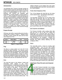
There are several registers in the HDLC Protocol
Controller accessible to the associated micro-
processor via the data bus. The addresses of these
registers are given in Table 1 and their functional
details are given below.
updated. When in internal 4.096 MHz timing mode,
the MT8952B must receive four falling edges of the
C4i clock before the Rx FIFO status bit will be
updated (see the section on Receive Operation -
Normal Packets).
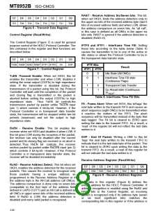
FIFO Status Register (Read):
Tx FIFO Status: These two bits (D3 and D2) indicate
the status of transmit FIFO as shown in Table 5.
This register (Figure 4) indicates the status of
transmit and receive FIFOs and the received byte as
described below.
Tx FIFO
Status Bits
Status
D3
0
D2
0
D7
D6
D5
D4
D3
D2
D1
D0
Tx FIFO Full
Rx Byte
Status
Rx FIFO
Status
Tx FIFO
Status
LOW
LOW
0
1
Greater than or equal to 5 bytes
Tx FIFO Empty
Figure 4 - FIFO Status Register
1
0
1
1
Less than or equal to 4 bytes
Rx Byte Status: These two bits (D7 and D6) indicate
the status of the received byte ready to be read from
the receive FIFO. The status is encoded as shown in
Table 3.
Table 5. Transmit FIFO Status
The Tx FIFO status bits are updated in the same
manner as the Rx FIFO bits, except that in external
timing mode, and in internal 2.048 Mbps timing
mode, the Tx FIFO status bits are updated after two
falling edges of the CKi or the C2i signal (see the
section on Transmit Operation - Normal Packets).
Rx Byte
Status Bits
Status
D7
0
D6
0
Packet Byte
First Byte
Receive Data Register (Read):
0
1
1
0
Last Byte (Good FCS)
Last Byte (Bad FCS)
Reading the Receive Data Register (Figure 5) puts
the first byte from the receive FIFO on the data bus.
The first bit of the data received on the serial input
(CDSTi) is considered to be the LSB and is available
on D0 of the data bus.
1
1
Table 3. Received Byte Status
Rx FIFO Status: These bits (D5 and D4) indicate the
status of receive FIFO as given by Table 4. The Rx
FIFO status bits are not updated immediately after
an access of the Rx FIFO (a read from the
microprocessor port, or a write from the serial port),
to avoid the existence of unrecoverable error
conditions.
D7
D6
D5
D4
D3
D2
D1
D0
RD7
RD6
RD5
RD4
RD3
RD2
RD1
RD0
Figure 5 - Receive Data Register
Transmit Data Register (Write):
When in external timing mode, the MT8952B must
receive two falling edges of the clock signal at the
CKi input before the Rx FIFO status bits will be
updated. When in internal 2.048 MHz timing mode,
the MT8952B must receive two falling edges of the
C2i clock before the Rx FIFO status bits will be
Writing to Transmit Data Register (Figure 6) puts the
data present on the data bus into the transmit FIFO.
The LSB (D0) is transmitted first.
3-67

 MITEL [ MITEL NETWORKS CORPORATION ]