MT8952B ISO-CMOS
RA6/7 - Receive Address Six/Seven bits: This bit,
when set HIGH, limits the address detection only to
the upper six bits of the received address byte (last 6
bits of received address field) and when LOW, allows
the address comparison on seven bits. An "all call",
in this case is defined as all ONEs in the upper six
bits only. RA6/7 is ignored if the address detection is
disabled (RxAD=0).
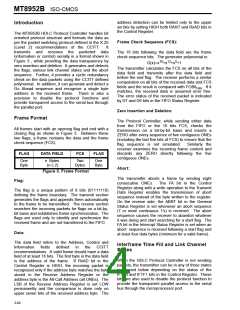
D7
D6
D5
D4
D3
D2
D1
D0
TD7
TD6
TD5
TD4
TD3
TD2
TD1
TD0
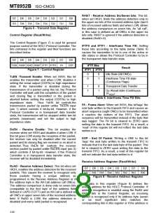
Figure 6 - Transmit Data Register
Control Register (Read/Write):
The Control Register (Figure 7) is used for general
purpose control of the HDLC Protocol Controller. The
bits contained in this register and their functions are
described below.
IFTF0 and IFTF1 - Interframe Time Fill: Setting
these bits according to the table below (Table 6)
causes the transmitter to be in one of the active or
idle states or allows the Protocol Controller to be in
the transparent data transfer state.
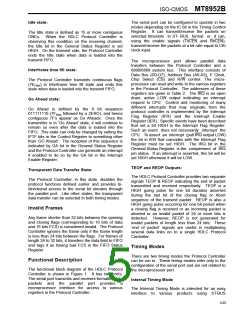
D7
D6
D5
D4
D3
D2
D1
D0
TxEN RxEN RxAD RA6/7 IFTF1 IFTF0
FA
EOP
IFTF Bits
Result
Figure 7 - Control Register
IFTF1
IFTF0
0
0
0
1
Idle State (All ONEs)
TxEN -Transmit Enable: When set HIGH, this bit
enables the transmitter and when LOW, disables it
setting the serial output (CDSTo) to high impedance
state. If the transmitter is disabled during the
transmission of a packet using this bit, the Protocol
Controller will wait until the completion of the packet
and closing flag is transmitted or the packet is
aborted before setting the output (CDSTo) to high
Interframe Time Fill state
(Continuous Flags)
1
1
0
1
Transparent Data Transfer
Go Ahead state (Continuous
7F
)
HEX
Table 6. Interframe Time Fill Bits
impedance state.
Thus TxEN bit controls the
FA - Frame Abort: When set HIGH, this bit’tags’ the
next byte written to the transmit FIFO and causes an
abort sequence (eight ONEs) to be transmitted when
it reaches the bottom of the FIFO. The abort
sequence will be transmitted instead of the byte that
was tagged. The FA bit is cleared to ZERO upon
writing the data to the transmit FIFO. As a result, a
‘read’ of this register bit will not reflect the last data
written to it.
transmission packet by packet unlike TxCEN input
(pin 1) which controls it bit-by-bit. However, if the
Protocol Controller is in transparent data transfer
state, the transmission will be stopped within two bit
periods (maximum) and set the output to high
impedance state.
RxEN - Receive Enable: This bit enables the
receiver when set HIGH and disables it when LOW. If
this bit goes LOW during the reception of the packet,
the receiver can only be disabled after the current
packet and its closing flag are received or an abort is
detected. Thus RxEN bit controls the receiver
section packet by packet unlike RxCEN input (pin 2)
which controls it bit-by-bit. However, if the Protocol
Controller is in transparent data transfer state, the
receiver will be disabled immediately.
EOP - End Of Packet: Writing a ONE to this bit
‘tags’ the next byte written to the transmit FIFO to
indicate that it is the last data byte of the packet. This
bit is cleared to ZERO upon writing the data to the
transmit FIFO. As a result, a read of this register bit
will not indicate the last data written to it.
Receive Address Register (Read/Write):
RxAD - Receive Address Detect: This bit when set
HIGH, enables the address detection for the received
packets. This causes the receiver to recognize only
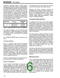
D7
D6
D5
D4
D3
D2
D1
D0
RA7
RA6
RA5
RA4
RA3
RA2
RA1
RA0
those packets having
a
unique address as
Figure 8 - Receive Address Register
programmed in the Receive Address Register or if
the address byte is the All-Call address (all ONEs).
The address comparison is done only on seven bits
(compatible to the first byte of the address field
defined in LAPD-CCITT) and an All-Call is defined as
all ONEs in upper seven bits of the received address
field. If RxAD is LOW, the address detection is
disabled and every valid packet is recognized.
The data in this register (Figure 8) defines the
unique address for the HDLC Protocol Controller. If
address recognition is enabled using the RxAD and
RA6/7 bits in the Control Register, an incoming
packet is recognized only if its address byte (seven
or six most significant bits) matches the
corresponding bits in this register or if the address is
3-68

 MITEL [ MITEL NETWORKS CORPORATION ]