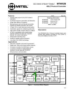
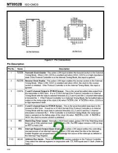
ISO-CMOS MT8952B
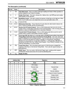
Pin Description (continued)
Pin No.
Name
Description
11
CS
Chip Select Input - This is an active LOW input enabling the Read or Write operation to
various registers in the Protocol Controller.
12
13
E
Enable Clock Input - This input activates the Address Bus and R/W input and enables
data transfers on the Data Bus.
R/W
Read/Write Control - This input controls the direction of data flow on the data bus. When
HIGH, the I/O buffer acts as an output driver and as an input buffer when LOW.
14
V
Ground (0 Volt).
SS
15-22
D0-D7 Bidirectional Data Bus - These Data Bus I/O ports allow the data transfer between the
HDLC Protocol Controller and the microprocessor.
23
REOP Receive End Of Packet (Output) - This is a HIGH going pulse that occurs for one bit
duration when a closing flag is detected on the incoming packets, or the incoming packet is
aborted, or when an invalid packet of 24 or more bits is received.
24
25
TEOP Transmit End Of Packet (Output) - This is a HIGH going pulse that occurs for one bit
duration when a packet is transmitted correctly or aborted.
CKi
Clock Input (Bit rate clock or 2 x bit rate clock in ST-BUS format while in the Internal
Timing Mode and bit rate Clock in the External Timing Mode) - This is the clock input
used for shifting in/out the formatted packets. It can be at bit rate (C2i) or twice the bit rate
(C4i) in ST-BUS format while the Protocol Controller is in the Internal Timing Mode.
Whether the clock should be C2i (typically 2.048 MHz) or C4i (typically 4.096 MHz) is
decided by the BRCK bit in the Timing Control Register. If the Protocol Controller is in the
External Timing Mode, it is at the bit rate.
26
F0i
Frame Pulse Input - This is the frame pulse input in ST-BUS format to establish the
beginning of the frame in the Internal Timing Mode. This is also the signal clocking the
watchdog timer.
27
28
RST
RESET Input - This is an active LOW Schmitt Trigger input, resetting all the registers
including the transmit and receive FIFOs and the watchdog timer.
V
Supply (5 Volts).
DD
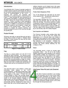
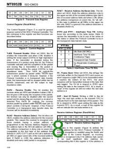
Address Bits
Registers
A3
A2
A1
A0
Read
Write
0
0
0
0
0
0
0
0
1
1
0
0
0
0
1
1
1
1
0
0
0
0
1
1
0
0
1
1
0
0
0
1
0
1
0
1
0
1
0
1
FIFO Status
Receive Data
-
Transmit Data
Control
Control
Receive Address
C-Channel Control (Transmit)
Timing Control
Receive Address
C-Channel Control (Transmit)
Timing Control
Watchdog Timer
Interrupt Enable
-
Interrupt Flag
Interrupt Enable
General Status
C-Channel Status (Receive)
-
Table 1. Register Addresses
3-63

 MITEL [ MITEL NETWORKS CORPORATION ]