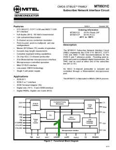
MT8931C
Pin Description (continued)
Pin #
Name
Description
DIP PLCC
9
16
17
R/W/WR Read/Write or Write Input: defines the data bus transfer as a read (R/W=1) or a write
(R/W=0) in Motorola bus mode. Redefined to WR in Intel bus mode.
10
DS/RD Data Strobe/Read Input: active high input indicates to the SNIC that valid data is on
the bus during a write operation or that the SNIC must output data during a read
operation in Motorola bus mode. Redefined to RD in Intel bus mode.
11
19
AS/ALE Address Strobe/Address Latch Enable Input: in Motorola bus mode the falling edge
is used to strobe the address into the SNIC during microprocessor access. Redefined
to ALE in Intel bus mode.
12
13
20
21
CS
Chip Select Input: active low, used to select the SNIC for microprocessor access.
IRQ
Interrupt Request (Open Drain Output): an output indicating an unmasked HDLC
interrupt. The interrupt remains active until the microprocessor clears it by reading the
HDLC Interrupt Status Register. This interrupt source is enabled with B2=0 of Master
Control Register.
New Data Available (Open Drain Output): an active low output signal indicating
availability of new data from the S-Bus. This signal is selected with B2=1 of Master
Control Register. This pin must be tied to VDD with a 10kΩ resistor.
NDA
14
22
VSS
Ground.
15- 24-26,
22 30-32,
34-35
AD0-7
Bidirectional Address/Data Bus: electrically and logically compatible to either Intel or
Motorola micro-bus specifications. If DS/RD is low on the rising edge of AS/ALE then
the chip operates to Motorola specs. If DS/RD is high on the rising edge of AS/ALE Intel
mode is selected. Taking Rsti low sets Motorola mode.
23
24
37
38
Rsti
Reset Input: Schmitt trigger reset input. If ’0’, sets all control registers to the default
conditions, resets activation state machines to the deactivated state, resets HDLC,
clears the HDLC FIFO‘s. Sets the microport to Motorola bus mode.
STAR/Rsto Star/Reset (Open Drain Output): 192kbit/s Rx data output fixed relative to the ST-
BUS timebase. A group of NTs, in fixed timing mode, can be wire or’ed together to
create a Star configuration. Active low reset output in TE mode indicating 128
consecutive marks have been received. Can be connected directly to Rsti to allow NT
to reset all TEs on the bus. This pin must be tied to VDD with a 10 kΩ resistor.
25
40
LRx
Receive Line Signal Input: this is a high impedance input for the pseudoternary line
signal to be connected to the line through a 2:1 ratio transformer. See Figures 20 and
21. A DC bias level on this input equal to V
must be maintained.
Bias
26
27
28
42
43
44
LTx
Transmit Line Signal Output: this is a current source output designed to drive a
nominal 50 ohm line through a 2:1 ratio transformer. See Figures 20 and 21.
VBias
Bias Voltage: analog ground for Tx and Rx transformers. This pin must be decoupled
to VDD through a 10µF capacitor with good high frequency characteristics.
VDD
NC
Power Supply Input.
No Connection.
1,5-6,10-
12,15,18,
23,27-
29, 33,
36, 39,
41
9-73

 MITEL [ MITEL NETWORKS CORPORATION ]