MT8931C
28
27
26
25
24
23
22
21
20
19
18
17
16
15
1
2
3
4
5
6
7
8
HALF
C4b
F0b
F0od
DSTi
VDD
VBias
LTx
LRx
STAR/Rsto
Rsti
AD7
AD6
AD5
AD4
40
44 43 42 41
6 5 4 3 2
1
NC
STAR/Rsto
Rsti
NC
AD7
AD6
NC
AD5
AD4
AD3
NC
7
F0od
DSTi
DSTo
39
8
38
37
36
35
34
33
32
31
30
29
DSTo
9
10
11
12
13
14
15
16
XTAL2/NC
XTAL1/NT
R/W/WR
DS/RD
AS/ALE
CS
NC
NC
NC
9
XTAL2/NC
10
11
12
13
14
XTAL1/NT
AD3
AD2
AD1
AD0
NC
R/W/WR
IRQ/NDA
VSS
DS/RD
17
18 19 20 21 22 23 24 25 26 27 28
28 PIN PDIP
44 PIN PLCC
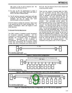
Figure 2 - Pin Connections
Pin Description
Pin #
Name
Description
DIP PLCC
1
2
HALF
HALF Input/Output: this is an input in NT mode and an output in TE mode identifying
which half of the S-interface frame is currently being written/read over the ST-BUS
(HALF = 0 sampled on the falling edge of C4b within the frame pulse low window,
identifies the information to be transmitted/received in the first half of the S-Bus frame
while HALF=1 identifies the information to be transmitted/received into the second half
of the S-Bus frame). Tying this pin to VSS or VDD in NT mode will allow the device to free
run. This signal can also be accessed from the ST-BUS C-channel.
2
3
4
3
4
7
C4b
F0b
4.096 MHz Clock: a 4.096 MHz ST-BUS Data Clock input in NT mode.
In TE mode an output 4.096 MHz clock phase-locked to the line data signal.
Frame Pulse: an active low frame pulse input indicating the beginning of active ST-
BUS channel times in NT mode. Frame pulse output in TE mode.
F0od
Delayed Frame Pulse Output: an active low delayed frame pulse output indicating
the end of active ST-BUS channels for this device. Can be used to daisy chain
to other ST-BUS devices to share an ST-BUS stream.
5
6
8
9
DSTi
DSTo
Data ST-BUS Input: a 2048 kbit/s serial PCM/data ST-BUS input with D, C, B1, and B2
channels assigned to the first four timeslots. These channels contain data to be
transmitted on the line and chip control information.
Data ST-BUS Output: a 2048 kbit/s serial PCM/data ST-BUS output with D, C, B1 and
B2 channels assigned to the first four timeslots, respectively. The remaining timeslots
are placed into high impedance. These channels contain data received from the line
and chip status information.
7
8
13
14
XTAL2/IC Crystal 2/Internal Connection: in TE mode, XTAL1 and XTAL2 are to be connected to
an external 4.096 MHz parallel resonant crystal for the on-chip oscillator.
If XTAL1 is connected directly to a 4.096 MHz clock, this pin must be left unconnected.
In NT mode, this pin must be left unconnected.
XTAL1/NT Crystal 1/Network Termination Mode Select Input: for TE mode mode selection, a
4.096 MHz crystal is to be connected between the XTAL1 and XTAL2 pins, or a 4.096
MHz clock can be connected directly to XTAL1. For NT mode selection, this pin must
be tied to VDD. A pull-up resistor is needed when driven by a TTL device.
9-72

 MITEL [ MITEL NETWORKS CORPORATION ]