TPU 3035, TPU 3040
PRELIMINARY DATA SHEET
pendent variations. Additionally characters from the G0
code table can be combined with diacritical marks from
the G2 code table (row 26). Thus it is not possible to sim-
ply transform the code tables into a continuous font
ROM without getting unused ROM space and multiple
defined character fonts.
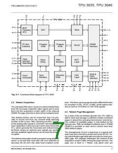
time faster than 120 ns. The data rate calculation al-
ready takes into account the required refresh cycles.
The DRAM interface has to handle 3 asynchronous data
streams. The CPU needs access to every memory loca-
tion of the DRAM. During VBI the slicer writes up to 22
teletext lines of 43 bytes into the acquisition scratch
memory. Alternatively the slicer can store MAC packets
of 90 bytes into the acquisition scratch. During text dis-
play the display controller copies teletext rows from dis-
play memory into its internal row buffer.
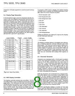
The character ROM is optimized by reorganizing the
code table structure of the WSTspecification. Thewhole
character font is subdivided into blocks of 32 characters
which are mapped to the WST character sets via a mask
programmable mapping ROM (see Fig. 4–5). The char-
acter set selection is done via software.
The lower data rate of the slow mode makes some re-
strictions necessary. With 6.1 Mbit/s it is no longer possi-
ble to run slicer and display in parallel. Only MAC packet
teletext can still be acquired asynchronously because of
the lower bit rate. VBI teletext can only be acquired while
the display controller is inactive (synchronous acquisi-
tion and display).
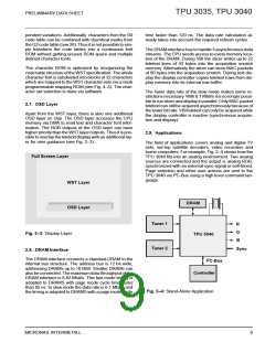
2.7. OSD Layer
Apart from the WST layer, there is also one additional
OSD layer on chip. The OSD layer accesses the CPU
memory via DMA to read text and character font infor-
mation. The RGB outputs of the OSD layer can have
higher priority than the WST layer outputs. Thus it is pos-
sibletooverlaytheteletextdisplaywithanadditionallay-
er for user guidance (see Fig. 2–3).
2.9. Applications
The field of applications covers analog and digital TV
sets, set-top satellite decoders, video recorders and
home computers. For example, Fig. 2–4 shows how the
TPU 3040 fits into an analog environment. Two analog
sources are connected and the output is analog RGB,
synchronized with an external sync signal or self-timed.
Page selection and other user actions are sent to the
Full Screen Layer
2
TPU 3040 via I C-Bus using a high level command lan-
guage.
WST Layer
OSD Layer
DRAM
Tuner 1
Tuner 2
R
G
B
Fig. 2–3: Display Layer
TPU 3040
Sync
2.8. DRAM Interface
The DRAM interface connects a standard DRAM to the
internal bus structure. The address bus is 12 bit wide,
addressing DRAMs up to 16 Mbit. Smaller DRAMs can
alsobeconnected. Themaximumdatathroughputofthe
DRAM interface is 8.82 Mbit/s. This fast mode timing is
adapted to DRAMS with page mode cycle time faster
than 85 ns. In slow mode the data rate is 6.1 Mbit/s and
the timing is adapted to DRAMS with a page mode cycle
2
I C-Bus
Controller
Fig. 2–4: Stand-Alone Application
MICRONAS INTERMETALL
9

 MICRONAS [ MICRONAS ]