TPU 3035, TPU 3040
PRELIMINARY DATA SHEET
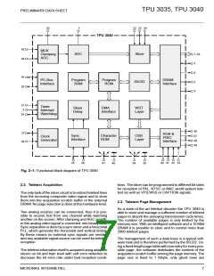
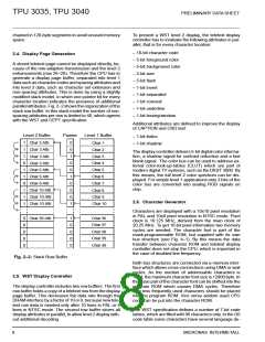
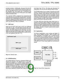
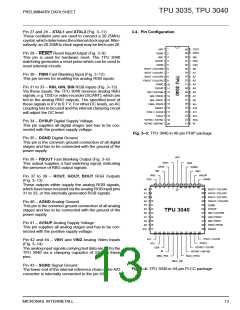
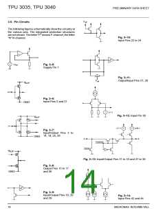
3.2. Pin Connections and Short Descriptions
Pin No.
44-pin PLCC
Pin No.
40-pin PDIP
Signal Name
Type
Symbol
1
2
1
40
39
38
37
36
35
34
33
32
31
30
29
28
27
26
25
24
23
22
21
–
Reference Voltage Top
Test Mode
Supply
Input
VRT
TEST
DATA
WE
3
DRAM Data
Input/Output
Output
Output
Output
Output
Output
Output
Output
Output
Output
Output
Output
Output
Output
Output
Output
Input/Output
Input/Output
Input
4
DRAM Write Enable
DRAM Row Address Strobe
DRAM Column Address Strobe
DRAM Address 0
DRAM Address 1
DRAM Address 2
DRAM Address 3
DRAM Address 4
DRAM Address 5
DRAM Address 6
DRAM Address 7
DRAM Address 8
DRAM Address 9
DRAM Address 10
DRAM Address 11
IIC Bus Clock
5
RAS
CAS
A0
6
7
8
A1
9
A2
10
11
12
13
14
15
16
17
18
19
20
21
22
23
24
25
A3
A4
A5
A6
A7
A8
A9
A10
A11
SCL
SDA
IR
IIC Bus Data
Infrared
MAC Paket Data
MAC VBI Data
Input
MAC_PAK
MAC_VBI
MAC_SYNC
–
Input
–
MAC Sync
Input
20
Horizontal Sync
Composite Sync 1
Main Sync
Input/Output
Output
Input
HSYNC
CSYNC1
MSYNC
26
19
Vertical Sync
Composite Sync 2
Input/Output
Output
VSYNC
CSYNC2
27
28
18
17
Crystal Oscillator Output
Output
XTAL2
Crystal Oscillator Input
Main Clock
Input
Input
XTAL1
CLK20
29
30
16
15
Reset
Input/Output
RESET
Fast Blank Input
Shadow
Priority Bus 0
Input
Output
Input/Output
FBIN
SHADOW
PRIO0
31
32
33
34
14
13
12
11
Analog Blue Input
Priority Bus 1
Input
Input/Output
BIN
PRIO1
Analog Green Input
Priority Bus 2
Input
Input/Output
GIN
PRIO2
Analog Red Input
Color Address Bus 4
Input
Output
RIN
COLOR4
Digital Supply Voltage
Supply
DVSUP
MICRONAS INTERMETALL
11

 MICRONAS [ MICRONAS ]