TPU 3035, TPU 3040
PRELIMINARY DATA SHEET
Pin 27 and 28 – XTAL1 and XTAL2 (Fig. 3–11)
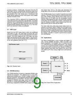
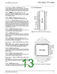
3.4. Pin Configuration
These oscillator pins are used to connect a 20.25MHz
crystal, which determines the internal clock signal. Alter-
natively, an 20.25MHz clock signal may be fed to pin 28.
1
VRT
SGND
40
39
38
37
36
35
34
33
32
31
30
29
28
27
26
25
TEST
DATA
2
Pin 29 – RESET Reset Input/Output (Fig. 3–9)
This pin is used for hardware reset. The TPU 3040
watchdog generates a reset pulse which can be used to
reset external circuits.
3
VIN1
WE
RAS
CAS
A0
AVSUP
4
AGND
5
ROUT / COLOR0
GOUT / COLOR1
BOUT / COLOR2
FBOUT / COLOR3
DGND
6
7
A1
Pin 30 – FBIN Fast Blanking Input (Fig. 3–12)
This pin serves for enabling the analog RGB inputs.
A2
8
A3
9
A4
10
11
12
13
14
15
16
Pin 31 to 33 – RIN, GIN, BIN RGB Inputs (Fig. 3–13)
Via these inputs, the TPU 3040 receives analog RBG
signals, e.g. OSD or video recorder (SCART), which are
fed to the analog RBG outputs. The specified level of
these signals is 0 V to 0.7 V. For other DC levels, an AC
coupling has to be used and the internal clamping circuit
will adjust the DC level.
DVSUP
A5
RIN / COLOR4
GIN / PRIO2
A6
A7
BIN / PRIO1
FBIN / PRIO0
RESET
A8
A9
A10
A11
SCL
SDA
IR
24
23
22
21
XTAL1 / CLK20
XTAL2
17
18
19
20
VSYNC / CSYNC
HSYNC / MSYNC
Pin 34 – DVSUP Digital Supply Voltage
This pin supplies all digital stages and has to be con-
nected with the positive supply voltage.
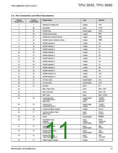
Fig. 3–3: TPU 3040 in 40-pin PDIP package
Pin 35 – DGND Digital Ground
This pin is the common ground connection of all digital
stages and has to be connected with the ground of the
power supply.
VRT
Pin 36 – FBOUT Fast Blanking Output (Fig. 3–8)
This output supplies a fast switching signal, indicating
the presence of RBG output signals.
TEST
DATA
WE
RAS
CAS
VIN2
SGND
VIN1
AVSUP
AGND
Pin 37 to 39 – ROUT, GOUT, BOUT RGB Outputs
(Fig. 3–13)
These outputs either supply the analog RGB signals,
which have been received via the analog RGB input pins
31 to 33, or the internally generated RGB signals.
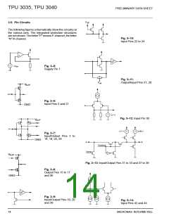
6
5
4
3
2
1 44 43 42 41 40
7
39
A0
A1
A2
ROUT / COLOR0
GOUT / COLOR1
BOUT / COLOR2
FBOUT / COLOR3
DGND
38
37
36
35
34
33
32
31
30
29
8
9
10
11
12
13
14
15
16
17
A3
A4
Pin 40 – AGND Analog Ground
This pin is the common ground connection of all analog
stages and has to be connected with the ground of the
power supply.
A5
A6
DVSUP
TPU 3040
RIN / COLOR4
GIN / PRIO2
BIN / PRIO1
FBIN / PRIO0
RESET
A7
A8
Pin 41 – AVSUP Analog Supply Voltage
This pin supplies all analog stages and has to be con-
nected with the positive supply voltage.
A9
A10
18 19 20 21 22 23 24 25 26 27 28
XTAL1 / CLK20
XTAL2
A11
SCL
SDA
Pin 42 and 44 – VIN1 and VIN2 Analog Video Inputs
(Fig. 3–14)
The analog input signals carrying text data are fed to the
TPU 3040 via a clamping capacitor of 33nF to these
pins.
VSYNC / CSYNC
HSYNC / MSYNC
IR
MAC_PAK
MAC_SYNC
MAC_VBI
Pin 43 – SGND Signal Ground
The lower end of the internal reference chain of the A/D
converter is internally connected to the pin 43.
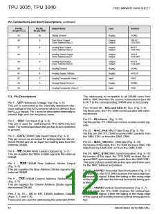
Fig. 3–4: TPU 3040 in 44-pin PLCC package
MICRONAS INTERMETALL
13

 MICRONAS [ MICRONAS ]