TPU 3035, TPU 3040
PRELIMINARY DATA SHEET
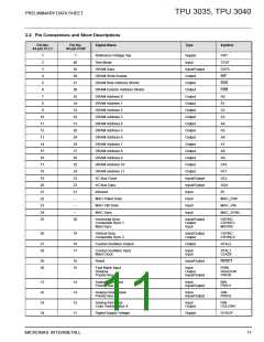
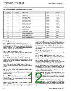
Pin Connections and Short Descriptions, continued
Pin No.
44-pin PLCC
Pin No.
40-pin PDIP
Signal Name
Type
Symbol
35
36
10
9
Digital Ground
Supply
DGND
Fast Blank Output
Color Address Bus 3
Output
Output
FBOUT
COLOR3
37
38
39
8
7
6
Analog Blue Output
Color Address Bus 2
Output
Output
BOUT
COLOR2
Analog Green Output
Color Address Bus 1
Output
Output
GOUT
COLOR1
Analog Red Output
Color Address Bus 0
Output
Output
ROUT
COLOR0
40
41
42
43
44
5
4
3
2
–
Analog Ground
Supply
Supply
Input
AGND
AVSUP
VIN1
Analog Supply Voltage
Analog Composite Video 1
Analog Signal Ground
Analog Composite Video 2
Supply
Input
SGND
VIN2
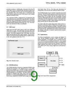
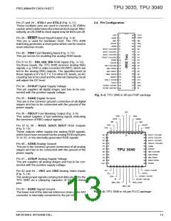
3.3. Pin Descriptions
The addressing is compatible to all DRAM sizes from
64K to 16M, therefore the correct connection of pins A8
to A11 to the corresponding DRAM pins is necessary.
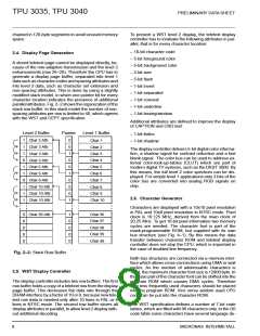
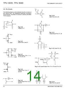
Pin 1 – VRT Reference Voltage Top (Fig. 3–5)
This pin is connected to the internally-stabilized refer-
ence voltage of the A/D converter which is derived from
Pins 19 and 20 – SCL and SDA IIC Bus (Fig. 3–9)
Via these pins, the TPU 3040 communicates with exter-
nal devices.
the V
supply. Pin 1 must be decoupled externally to
ASUP
prevent high and low frequency noise.
Pin 21 – IR Infrared (Fig. 3–10)
ViathispintheTPU3040canreceiveremotecontrolsig-
nals.
Pin 2 – TEST Test Input (Fig. 3–6)
This pin is used for switching the TPU 3040 into test
mode. For normal operation this pin has to be connected
to ground.
Pin 22 – MAC_PAK MAC Paket Data (Fig. 3–10)
Via this pin, the TPU 3040 receives MAC packets from
the DMA 2381 or from the DMA 2386.
Pin 3 – DATA DRAM Data Input/Output (Fig. 3–7)
This pin serves as an output for writing data into the ex-
ternal DRAM and as an input for reading data from the
external DRAM.
Pin 23 – MAC_VBI MAC VBI Data (Fig. 3–10)
By means of this input, the TPU 3040 receives MAC VBI
data from the DMA 2381 or from the DMA 2386.
Pin 4 – WE DRAM Write Enable Output (Fig. 3–7)
This pin supplies the Write Enable signal to the external
DRAM.
Pin 24 – MAC_SYNC MAC Synchronization (Fig. 3–10)
By means of this input, the TPU 3040 receives the re-
quired MAC synchronization pulse from the DMA 2381.
This sync pulse is used both as line sync and frame sync
for the MAC teletext acquisition.
Pin 5 – RAS DRAM Row Address Strobe Output
(Fig. 3–7)
This pin supplies the Row Address Strobe signal to the
external DRAM.
Pin 25 – HSYNC Horizontal Synchronization (Fig. 3–7)
Via this input, the TPU 3040 receives the horizontal syn-
chronization signal. Either the falling or the rising edge
of this signal will start the internal horizontal timing gen-
eration.
Pin 6 – CAS DRAM Column Address Strobe Output
(Fig. 3–7)
This pin supplies the Column Address Strobe signal to
the external DRAM.
Pin 26 – VSYNC Vertical Synchronization (Fig. 3–7)
Via this input, the TPU 3040 receives the vertical syn-
chronization signal. Either the falling or the rising edge
of this signal will start the internal vertical timing genera-
tion.
Pins 7 to 18 – A0 to A11 DRAM Address Outputs
(Figs. 3–7 and 3–8)
These pins are used for addressing the external DRAM.
12
MICRONAS INTERMETALL

 MICRONAS [ MICRONAS ]