‡
Pre lim in a ry
MT9V012 - 1/6-In ch VGA CMOS Dig it a l Im a g e Se n so r
Ele ct rica l Sp e cifica t io n s
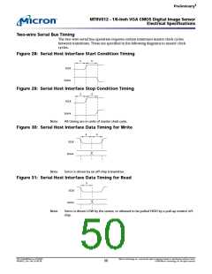
Tw o -w ire Se ria l Bu s Tim in g
The two-wire serial bus operation requires certain minimum master clock cycles
between transitions. These are specified in the following diagrams in master clock
cycles.
Fig u re 28: Se ria l Ho st In t e rfa ce St a rt Co n d it io n Tim in g
5
4
SCLK
SDATA
Fig u re 29: Se ria l Ho st In t e rfa ce St o p Co n d it io n Tim in g
5
4
SCLK
SDATA
Note:
All timing are in units of master clock cycle.
Fig u re 30: Se ria l Ho st In t e rfa ce Da t a Tim in g fo r Writ e
4
4
SCLK
SDATA
Note:
SDATA is driven by an off-chip transmitter.
Fig u re 31: Se ria l Ho st In t e rfa ce Da t a Tim in g fo r Re a d
5
SCLK
SDATA
Note:
SDATA is driven LOW by the sensor, or allowed to be pulled HIGH by a pull-up resistor off-
chip.
PDF: 814eb99f/Source: 8175e929
MT9V012_2.fm - Rev. B 2/05 EN
Micron Technology, Inc., reserves the right to change products or specifications without notice.
50
©2004 Micron Technology, Inc. All rights reserved.

 MICRON [ MICRON TECHNOLOGY ]