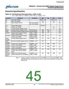
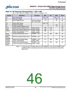
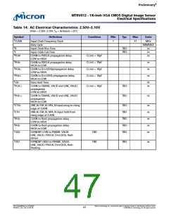
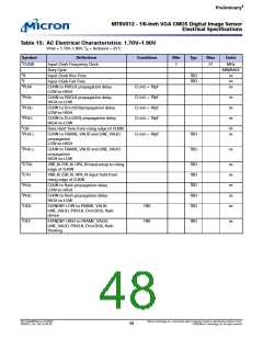
‡
Pre lim in a ry
MT9V012 - 1/6-In ch VGA CMOS Dig it a l Im a g e Se n so r
Ele ct rica l Sp e cifica t io n s
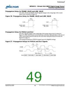
Pro p a g a t io n De la y fo r FRAME_VALID a n d LINE_VALID
The LINE_VALID and FRAME_VALID signals change on the rising edge of the master
input clock, as shown in Figure 26.
Fig u re 26: Pro p a g a t io n De la y fo r FRAME_VALID a n d LINE_VALID
t
t
PHLF,L
PLHF,L
CLKIN
CLKIN
FRAME_VALID
LINE_VALID
FRAME_VALID
LINE_VALID
Pro p a g a t io n De la y fo r PIXCLK a n d DOUT
The DOUT signals change on the rising edge of the master input clock, as shown in
Figure 27. LINE_VALID asserts at the same time as the first valid pixel data, at the start of
a line, and remains asserted until the end of the final valid pixel data for the line (see
Figure 8 on page 11).
The timing and behavior of PIXCLK depend upon the Reg0x0A settings.
Fig u re 27: Pro p a g a t io n De la ys fo r PIXCLK a n d DOUT Sig n a ls
t
t
R
F
t
CLKIN
t
PLHP
PHLP
PIXCLK
t
PHLD, t
t
PLHD
OH
DOUT (9:0)
DOUT (9:0)
DOUT (9:0)
DOUT (9:0)
DOUT (9:0)
PDF: 814eb99f/Source: 8175e929
MT9V012_2.fm - Rev. B 2/05 EN
Micron Technology, Inc., reserves the right to change products or specifications without notice.
©2004 Micron Technology, Inc. All rights reserved.
49

 MICRON [ MICRON TECHNOLOGY ]