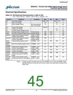
‡
Pre lim in a ry
MT9V012 - 1/6-In ch VGA CMOS Dig it a l Im a g e Se n so r
Ele ct rica l Sp e cifica t io n s
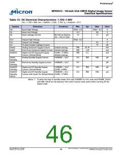
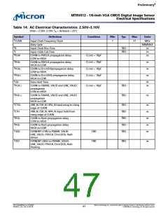
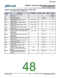
Ta b le 13: DC Ele ct rica l Ch a ra ct e rist ics: 1.70V–1.90V
VDD = 1.70V–1.90V; VAA = VAAPIX = 2.50V - 3.10V; TA = Ambient = 25°C
Sym b o l
De fin it io n
Input High Voltage
Co n d it io n
Min
Typ
Ma x
Un it s
VPWR - 0.3
-0.3
VPWR + 0.3
V
V
VIH
0.8
15
VIL
IIN
Input Low Voltage
-15
µA
Input Leakage Current
No Pull-up Resistor;
VIN = VDD or DGND
VPWR - 0.2
V
VOH
Output High Voltage
0.2
15
V
VOL
Output Low Voltage
µA
mA
mA
mA
IOZ
Tri-state Output Leakage Current
Analog Quiescent Supply Current
TBD
TBD
TBD
25.76
1.39
2.5
IPWRA
IPWRP
IPWRIOD
Default settings
Pixel Array Quiescent Supply Current Default settings
Digital and I/O Quiescent Supply
Current, Default Mode
CLKIN = 27 MHz;
default settings
1
0.0
0.0
0.0
0.0
TBD
TBD
µA
µA
µA
µA
IPWRA
Standby
Analog Standby Supply Current
STANDBY = VDD
1
IPWRP
Standby
Pixel Array Standby Supply Current
STANDBY = VDD
1
TBD
TBD
TBD
TBD
IPWRIOD
Standby
Digital and I/O Standby Supply
Current, Default Mode
STANDBY = VDD ,
CLKIN = 0 MHz
IPWRIOD
Standby
ClkOn
Digital and I/O Standby Supply
STANDBY = VDD,
Current with Clock On, Default Mode CLKIN = 27 MHz
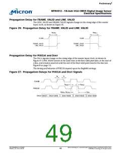
Notes: 1. To place the chip in standby mode, first raise STANDBY to VDD, wait until FRAME_VALID
and LINE_VALID are de-asserted, then wait 2 master clock cycles before turning off the
master clock.
PDF: 814eb99f/Source: 8175e929
MT9V012_2.fm - Rev. B 2/05 EN
Micron Technology, Inc., reserves the right to change products or specifications without notice.
46
©2004 Micron Technology, Inc. All rights reserved.

 MICRON [ MICRON TECHNOLOGY ]