ADVANCE
128Mb: x16, x32
MOBILE SDRAM
NOTES
t
1. All voltages referenced to VSS.
2. This parameter is sampled. VDD, VDDQ = +3.3V;
14. Timing actually specified by CKS; clock(s) specified
as a reference only at minimum cycle rate.
t
t
f = 1 MHz, T = 25°C; pin under test biased at 1.4V.
15. Timing actually specified by WR plus RP; clock(s)
specified as a reference only at minimum cycle rate.
A
3. IDD is dependent on output loading and cycle rates.
Specified values are obtained with minimum cycle
time and the outputs open.
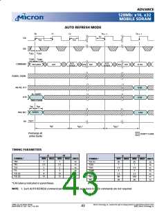
4. Enables on-chip refresh and address counters.
5. The minimum specifications are used only to
indicate cycle time at which proper operation over
t
16. Timing actually specified by WR.
17. Required clocks are specified by JEDEC functionality
and are not dependent on any timing parameter.
18. The IDD current will increase or decrease propor-
tionally according to the amount of frequency alter-
ation for the test condition.
the full temperature range (-40°C ≤ T ≤ +85°C for
IT parts) is ensured.
A
19. Address transitions average one transition every two
clocks.
6. An initial pause of 100µs is required after power-up,
followed by two AUTO REFRESH commands, before
proper device operation is ensured. (VDD and VDDQ
must be powered up simultaneously. VSS and VSSQ
mustbeatsamepotential.)ThetwoAUTOREFRESH
command wake-ups should be repeated any time
20. CLK must be toggled a minimum of two times during
this period.
t
t
21. Based on CK =8ns for -8 and CK =10ns for -10.
22. VIH overshoot: VIH (MAX) = VDDQ + 2V for a pulse width
≤ 3ns, and the pulse width cannot be greater than one
third of the cycle rate. VIL undershoot: VIL (MIN) = -2V
for a pulse width ≤ 3ns.
t
the REF refresh requirement is exceeded.
t
7. AC characteristics assume T = 1ns.
8. In addition to meeting the transition rate specifica-
tion, theclockandCKEmusttransitbetweenVIH and
VIL (or between VIL and VIH) in a monotonic manner.
9. Outputs measured for 3.3V at1.5V or 2.5V at 1.25V
with equivalent load:
23. The clock frequency must remain constant (stable
clock is defined as a signal cycling within timing
constraints specified for the clock pin) during access
t
or precharge states (READ, WRITE, including WR,
and PRECHARGE commands). CKE may be used to
reduce the data rate.
24. Auto precharge mode only. The precharge timing
Q
t
budget ( RP) begins at 7ns for -8 after the first clock
30pF
delay, after the last WRITE is executed. May not ex-
ceed limit set for precharge mode.
25. Precharge mode only.
26. JEDEC and PC100 specify three clocks.
27. AC for -8 at CL = 3 with no load is 7ns and is guaran-
t
10. HZ defines the time at which the output achieves the
t
open circuit condition; it is not a reference to VOH or
VOL. The last valid data element will meet OH before
going High-Z.
teed by design.
t
28. Parameter guaranteed by design.
29. PC100 specifies a maximum of 4pF.
30. PC100 specifies a maximum of 5pF.
31. PC100 specifies a maximum of 6.5pF.
11. AC timing and IDD tests have VIL and VIH, with timing
referenced to VIH/2 = crossover point. If the input
transition time is longer than t (MAX), then the
t
T
32. For -8, CL = 2 and CK = 10ns; for -10, CL = 3 and
timing is referenced at VIL (MAX) and VIH (MIN) and
no longer at the VIH/2 crossover point.
12. Other input signals are allowed to transition no more
than once every two clocks and are otherwise at valid
VIH or VIL levels.
t
CK =10ns.
33. CKE is HIGH during refresh command period
t
RFC (MIN) else CKE is LOW. The IDD6 limit is actu-
ally a nominal value and does not result in a fail
value.
13. IDD specifications are tested after the device is prop-
erly initialized.
128Mb: x16, x32 Mobile SDRAM
MobileY95W_3V_F.p65 – Rev. F; Pub. 9/02
Micron Technology, Inc., reserves the right to change products or specifications without notice.
©2002, Micron Technology, Inc.
39

 MICRON [ MICRON TECHNOLOGY ]