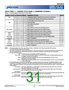
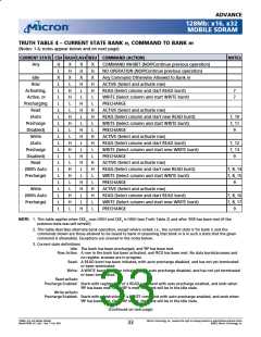
ADVANCE
128Mb: x16, x32
MOBILE SDRAM
*Stresses greater than those listed under “Absolute Maxi-
mum Ratings” may cause permanent damage to the de-
vice. This is a stress rating only, and functional operation
of the device at these or any other conditions above those
indicated in the operational sections of this specification
is not implied. Exposure to absolute maximum rating
conditions for extended periods may affect reliability.
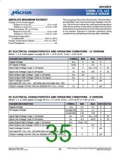
ABSOLUTE MAXIMUM RATINGS*
Voltage on VDD/VDDQ Supply
Relative to VSS(3.3V) ............................. -1V to +4.6V
Relative to VSS(2.5V) ......................... -0.5V to +3.6V
Voltage on Inputs, NC or I/O Pins
Relative to VSS(3.3V) ............................. -1V to +4.6V
Relative to VSS(2.5V) ......................... -0.5V to +3.6V
Operating Temperature,
T
(Industrial) ....................................... -40°C to +85°C
A
Storage Temperature (plastic) ................ -55°C to +150°C
Power Dissipation ..........................................................1W
DC ELECTRICAL CHARACTERISTICS AND OPERATING CONDITIONS - LC VERSION
(Notes: 1, 5, 6; notes appear on page 39; VDD = +3.3V 0.3V, VDDQ = +3.3V 0.3V
PARAMETER/CONDITION
Supply Voltage
SYMBOL
VDD
MIN
MAX UNITS NOTES
3
3
2
3.6
3.6
V
V
V
I/O Supply Voltage
VDDQ
VIH
Input High Voltage: Logic 1; All inputs
VDD + 0.3
22
22
Input Low Voltage: Logic 0; All inputs
VIL
VOH
VOL
II
-0.3
2.4
–
0.8
–
V
V
Data Output High Voltage: Logic 1; All inputs
Data Output LOW Voltage: LOGIC 0; All inputs
0.4
5
V
Input Leakage Current:
-5
µA
Any Input 0V ≤ VIN ≤ VDD (All other pins not under test = 0V)
Output Leakage Current: DQs are disabled; 0V ≤ VOUT ≤ VDDQ
IOZ
-5
5
µA
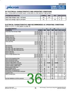
DC ELECTRICAL CHARACTERISTICS AND OPERATING CONDITIONS - V VERSION
(Notes: 1, 5, 6; notes appear on page 39; VDD = 2.5 0.2V, VDDQ = +2.5V 0.2V or +1.8V 0.15V )
PARAMETER/CONDITION
Supply Voltage
SYMBOL
MIN
2.3
MAX UNITS NOTES
VDD
2.7
2.7
V
V
I/O Supply Voltage
VDDQ(2.5V)
2.3
VDDQ(1.8V)
1.65
1.25
-0.3
1.95
VDD + 0.3
+0.55
–
V
Input High Voltage: Logic 1; All inputs
VIH
VIL
VOH
VOL
II
V
22
22
Input Low Voltage: Logic 0; All inputs
V
Data Output High Voltage: Logic 1; All inputs
Data Output Low Voltage: LOGIC 0; All inputs
Input Leakage Current:
VDDQ - 0.2
–
V
0.2
V
-2
2
µA
Any input 0V ≤ VIN ≤ VDD (All other pins not under test = 0V)
Output Leakage Current: DQs are disabled; 0V ≤ VOUT ≤ VDDQ
IOZ
-5
5
µA
128Mb: x16, x32 Mobile SDRAM
MobileY95W_3V_F.p65 – Rev. F; Pub. 9/02
Micron Technology, Inc., reserves the right to change products or specifications without notice.
©2002, Micron Technology, Inc.
35

 MICRON [ MICRON TECHNOLOGY ]