ADVANCE
128Mb: x16, x32
MOBILE SDRAM
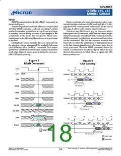
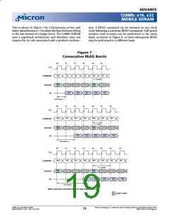
This is shown in Figure 7 for CAS latencies of two and
three; data element n + 3 is either the last of a burst of four
or the last desired of a longer burst. The 128Mb SDRAM
uses a pipelined architecture and therefore does not
require the 2n rule associated with a prefetch architec-
ture. A READ command can be initiated on any clock
cycle following a previous READ command. Full-speed
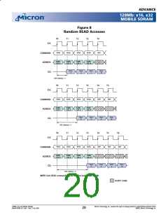
random read accesses can be performed to the same
bank, as shown in Figure 8, or each subsequent READ
may be performed to a different bank.
Figure 7
Consecutive READ Bursts
T0
T1
T2
T3
T4
T5
CLK
READ
NOP
NOP
NOP
READ
NOP
COMMAND
X = 0 cycles
BANK,
COL n
BANK,
COL b
ADDRESS
DQ
D
OUT
D
n + 1
OUT
D
n + 2
OUT
DOUT
D
OUT
n
n + 3
b
CAS Latency = 1
T0
T1
T2
T3
T4
T5
T6
CLK
READ
NOP
NOP
NOP
READ
NOP
NOP
COMMAND
X = 1 cycle
BANK,
COL n
BANK,
COL b
ADDRESS
DQ
D
OUT
D
n + 1
OUT
DOUT
D
n + 3
OUT
D
OUT
n
n + 2
b
CAS Latency = 2
T1
T0
T2
T3
T4
T5
T6
T7
CLK
READ
NOP
NOP
NOP
READ
NOP
NOP
NOP
COMMAND
X = 2 cycles
BANK,
COL n
BANK,
COL b
ADDRESS
DQ
D
OUT
DOUT
D
n + 2
OUT
D
n + 3
OUT
DOUT
b
n
n + 1
CAS Latency = 3
NOTE: Each READ command may be to either bank. DQM is LOW.
DON’T CARE
128Mb: x16, x32 Mobile SDRAM
MobileY95W_3V_F.p65 – Rev. F; Pub. 9/02
Micron Technology, Inc., reserves the right to change products or specifications without notice.
©2002, Micron Technology, Inc.
19

 MICRON [ MICRON TECHNOLOGY ]