1Gb: x4, x8, x16 DDR2 SDRAM
Input Electrical Characteristics and Operating Conditions
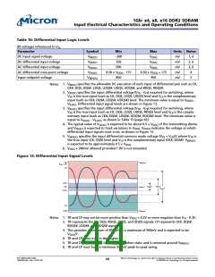
Table 16: Differential Input Logic Levels
All voltages referenced to VSS
Parameter
Symbol
VIN(DC)
VID(DC)
VID(AC)
VIX(AC)
VMP(DC)
Min
Max
VDDQ
Units Notes
DC input signal voltage
–300
mV
mV
mV
mV
mV
1, 6
2, 6
3, 6
4
DC differential input voltage
AC differential input voltage
AC differential cross-point voltage
Input midpoint voltage
250
500
VDDQ
VDDQ
0.50 × VDDQ - 175
850
0.50 × VDDQ + 175
950
5
1. VIN(DC) specifies the allowable DC execution of each input of differential pair such as CK,
CK#, DQS, DQS#, LDQS, LDQS#, UDQS, UDQS#, and RDQS, RDQS#.
Notes:
2. VID(DC) specifies the input differential voltage |VTR - VCP| required for switching, where
VTR is the true input (such as CK, DQS, LDQS, UDQS) level and VCP is the complementary
input (such as CK#, DQS#, LDQS#, UDQS#) level. The minimum value is equal to VIH(DC)
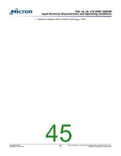
VIL(DC). Differential input signal levels are shown in Figure 13.
-
3. VID(AC) specifies the input differential voltage |VTR - VCP| required for switching, where
VTR is the true input (such as CK, DQS, LDQS, UDQS, RDQS) level and VCP is the comple-
mentary input (such as CK#, DQS#, LDQS#, UDQS#, RDQS#) level. The minimum value is
equal to VIH(AC) - VIL(AC), as shown in Table 15 (page 43).
4. The typical value of VIX(AC) is expected to be about 0.5 × VDDQ of the transmitting device
and VIX(AC) is expected to track variations in VDDQ. VIX(AC) indicates the voltage at which
differential input signals must cross, as shown in Figure 13.
5. VMP(DC) specifies the input differential common mode voltage (VTR + VCP)/2 where VTR is
the true input (CK, DQS) level and VCP is the complementary input (CK#, DQS#). VMP(DC)
is expected to be approximately 0.5 × VDDQ
.
6. VDDQ + 300mV allowed provided 1.9V is not exceeded.
Figure 13: Differential Input Signal Levels
1
2.1V
VIN(DC)max
VDDQ = 1.8V
2
CP
1.075V
0.9V
X
5
4
3
VID(DC)
VIX(AC)
VMP(DC)
6
VID(AC)
0.725V
X
2
TR
1
VIN(DC)min
–0.30V
1. TR and CP may not be more positive than VDDQ + 0.3V or more negative than VSS - 0.3V.
Notes:
2. TR represents the CK, DQS, RDQS, LDQS, and UDQS signals; CP represents CK#, DQS#,
RDQS#, LDQS#, and UDQS# signals.
3. This provides a minimum of 850mV to a maximum of 950mV and is expected to be
VDDQ/2.
4. TR and CP must cross in this region.
5. TR and CP must meet at least VID(DC)min when static and is centered around VMP(DC)
6. TR and CP must have a minimum 500mV peak-to-peak swing.
.
PDF: 09005aef821ae8bf
1GbDDR2.pdf – Rev. T 02/10 EN
Micron Technology, Inc. reserves the right to change products or specifications without notice.
44
© 2004 Micron Technology, Inc. All rights reserved.

 MICRON [ MICRON TECHNOLOGY ]